Datasheet 搜索 > 稳压芯片 > Linear Technology(凌力尔特) > LT1370IT7#PBF 数据手册 > LT1370IT7#PBF 数据手册 5/16 页

¥ 59.635
LT1370IT7#PBF 数据手册 - Linear Technology(凌力尔特)
制造商:
Linear Technology(凌力尔特)
分类:
稳压芯片
封装:
TO-220-7
描述:
开关稳压器 500kHz Hi Eff 6A Sw Reg
Pictures:
3D模型
符号图
焊盘图
引脚图
产品图
页面导航:
导航目录
LT1370IT7#PBF数据手册
Page:
of 16 Go
若手册格式错乱,请下载阅览PDF原文件
5
LT1370
sn1370 1370fs
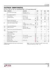
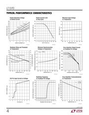
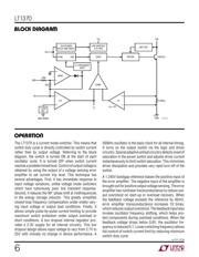
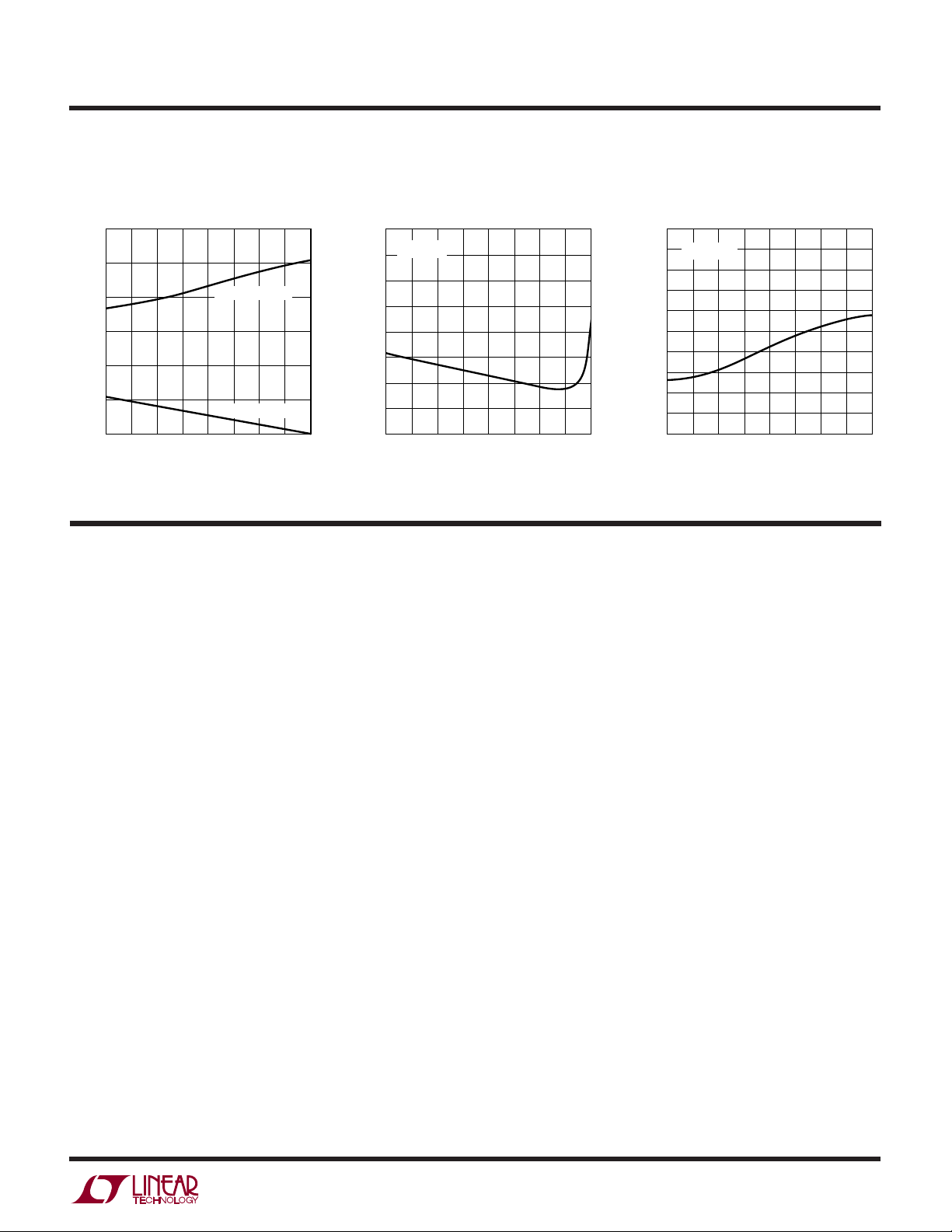
TYPICAL PERFORMANCE CHARACTERISTICS
U
W
TEMPERATURE (°C)
–50
FEEDBACK INPUT CURRENT (nA)
400
500
600
150
LT1370 • G11
300
200
0
0
50
100
100
800
700
–25
25
75
125
V
FB
=V
REF
Feedback Input Current
vs Temperature
TEMPERATURE (°C)
–50
–50
NEGATIVE FEEDBACK INPUT CURRENT (µA)
–30
0
0
50
75
LT1370 • G12
–40
–10
–20
–25 25
100
125
150
V
NFB
=V
NFR
Negative Feedback Input Current
vs Temperature
V
C
Pin Threshold and High
Clamp Voltage vs Temperature
TEMPERATURE (°C)
–50
1.0
V
C
VOLTAGE (V)
1.4
2.2
0
50
75
LT1370 • G10
1.2
1.8
2.0
1.6
–25 25
100
125
150
V
C
HIGH CLAMP
V
C
THRESHOLD
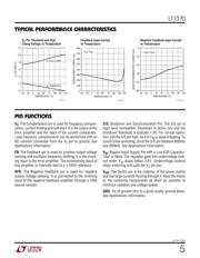
PIN FUNCTIONS
UUU
V
C
: The Compensation pin is used for frequency compen-
sation, current limiting and soft start. It is the output of the
error amplifier and the input of the current comparator.
Loop frequency compensation can be performed with an
RC network connected from the V
C
pin to ground. See
Applications Information.
FB: T
he Feedback pin is used for positive output voltage
sensing and oscillator frequency shifting. It is the invert-
ing input to the error amplifier. The noninverting input of
this amplifier is internally tied to a 1.245V reference.
NFB: The Negative Feedback pin is used for negative
output voltage sensing. It is connected to the inverting
input of the negative feedback amplifier through a 100k
source resistor.
S/S: Shutdown and Synchronization Pin. The S/S pin is
logic level compatible. Shutdown is active low and the
shutdown threshold is typically 1.3V. For normal opera-
tion, pull the S/S pin high, tie it to V
IN
or leave it floating. To
synchronize switching, drive the S/S pin between 600kHz
and 800kHz. See Applications Information.
V
IN
: Bypass Input Supply Pin with a Low ESR Capacitor,
10µF or More. The regulator goes into undervoltage lock-
out when V
IN
drops below 2.5V. Undervoltage lockout
stops switching and pulls the V
C
pin low.
V
SW
: The Switch pin is the collector of the power switch
and has large currents flowing through it. Keep the traces
to the switching components as short as possible to
minimize radiation and voltage spikes.
GND: Tie all ground pins to a good quality ground plane.
See Applications Information.
器件 Datasheet 文档搜索
AiEMA 数据库涵盖高达 72,405,303 个元件的数据手册,每天更新 5,000 多个 PDF 文件
