Datasheet 搜索 > 稳压芯片 > Linear Technology(凌力尔特) > LT1370IT7#PBF 数据手册 > LT1370IT7#PBF 数据手册 6/16 页

¥ 59.635
LT1370IT7#PBF 数据手册 - Linear Technology(凌力尔特)
制造商:
Linear Technology(凌力尔特)
分类:
稳压芯片
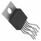
封装:
TO-220-7
描述:
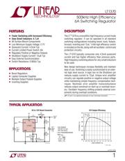
开关稳压器 500kHz Hi Eff 6A Sw Reg
Pictures:
3D模型
符号图
焊盘图
引脚图
产品图
页面导航:
导航目录
LT1370IT7#PBF数据手册
Page:
of 16 Go
若手册格式错乱,请下载阅览PDF原文件
6
LT1370
sn1370 1370fs
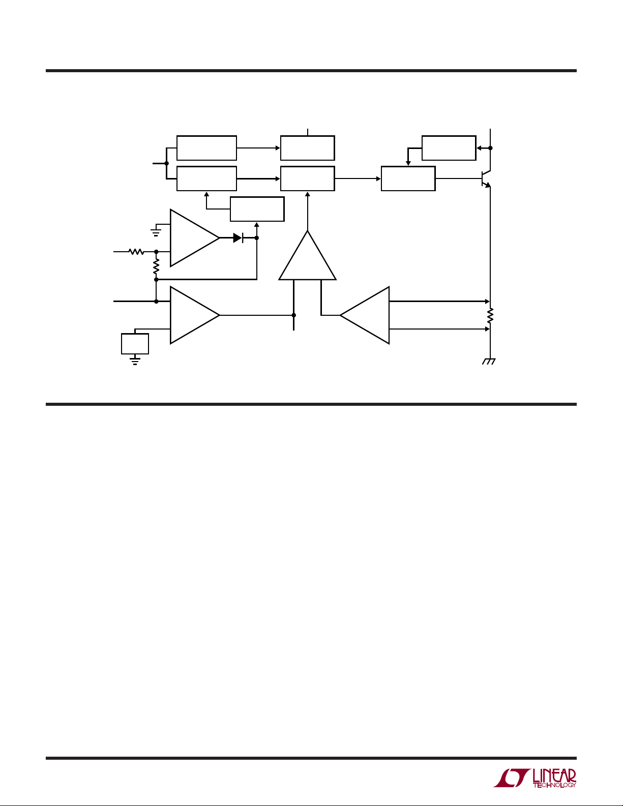
BLOCK DIAGRAM
W
OPERATION
U
The LT1370 is a current mode switcher. This means that
switch duty cycle is directly controlled by switch current
rather than by output voltage. Referring to the block
diagram, the switch is turned ON at the start of each
oscillator cycle. It is turned OFF when switch current
reaches a predetermined level. Control of output voltage is
obtained by using the output of a voltage sensing error
amplifier to set current trip level. This technique has
several advantages. First, it has immediate response to
input voltage variations, unlike voltage mode switchers
which have notoriously poor line transient response.
Second, it reduces the 90° phase shift at midfrequencies
in the energy storage inductor. This greatly simplifies
closed-loop frequency compensation under widely vary-
ing input voltage or output load conditions. Finally, it
allows simple pulse-by-pulse current limiting to provide
maximum switch protection under output overload or
short conditions. A low dropout internal regulator pro-
vides a 2.3V supply for all internal circuitry. This low
dropout design allows input voltage to vary from 2.7V to
25V with virtually no change in device performance. A
500kHz oscillator is the basic clock for all internal timing.
It turns on the output switch via the logic and driver
circuitry. Special adaptive antisat circuitry detects onset of
saturation in the power switch and adjusts driver current
instantaneously to limit switch saturation. This minimizes
driver dissipation and provides very rapid turn-off of the
switch.
A 1.245V bandgap reference biases the positive input of
the error amplifier. The negative input of the amplifier is
brought out for positive output voltage sensing. The error
amplifier has nonlinear transconductance to reduce out-
put overshoot on start-up or overload recovery. When
the feedback voltage exceeds the reference by 40mV,
error amplifier transconductance increases 10 times,
which reduces output overshoot. The feedback input also
invokes oscillator frequency shifting, which helps pro-
tect components during overload conditions. When the
feedback voltage drops below 0.6V, the oscillator fre-
quency is reduced 5:1. Lower switching frequency allows
full control of switch current limit by reducing minimum
switch duty cycle.
–
+
NFBA
NFB
S/S
FB
100k
50k
0.005Ω
–
+
EA
V
C
V
IN
GND
LT1370 • BD
GND SENSE
1.245V
REF
5:1 FREQUENCY
SHIFT
OSCSYNC
SHUTDOWN
DELAY AND RESET
LOW DROPOUT
2.3V REG
ANTI-SAT
LOGIC DRIVER
SW
SWITCH
–
+
IA
A
V
≈ 20
COMP
器件 Datasheet 文档搜索
AiEMA 数据库涵盖高达 72,405,303 个元件的数据手册,每天更新 5,000 多个 PDF 文件
