Datasheet 搜索 > Linear Technology(凌力尔特) > LTC4364HMS-2#TRPBF 数据手册 > LTC4364HMS-2#TRPBF 数据手册 14/24 页
 器件3D模型
¥ 46.372
LTC4364HMS-2#TRPBF 数据手册 - Linear Technology(凌力尔特)
制造商:
Linear Technology(凌力尔特)
封装:
MSOP-16
Pictures:
3D模型
符号图
焊盘图
引脚图
产品图
页面导航:
引脚图在P7P8Hot
典型应用电路图在P1P19P20P21P24
原理图在P9
封装尺寸在P21
焊盘布局在P22P23
型号编码规则在P3
标记信息在P3
封装信息在P3
技术参数、封装参数在P4
应用领域在P1P7P8P11P12P13P14P15P16P17P18P19
电气规格在P3P4P5P6P12
导航目录
LTC4364HMS-2#TRPBF数据手册
Page:
of 24 Go
若手册格式错乱,请下载阅览PDF原文件
LTC4364-1/LTC4364-2
14
436412f
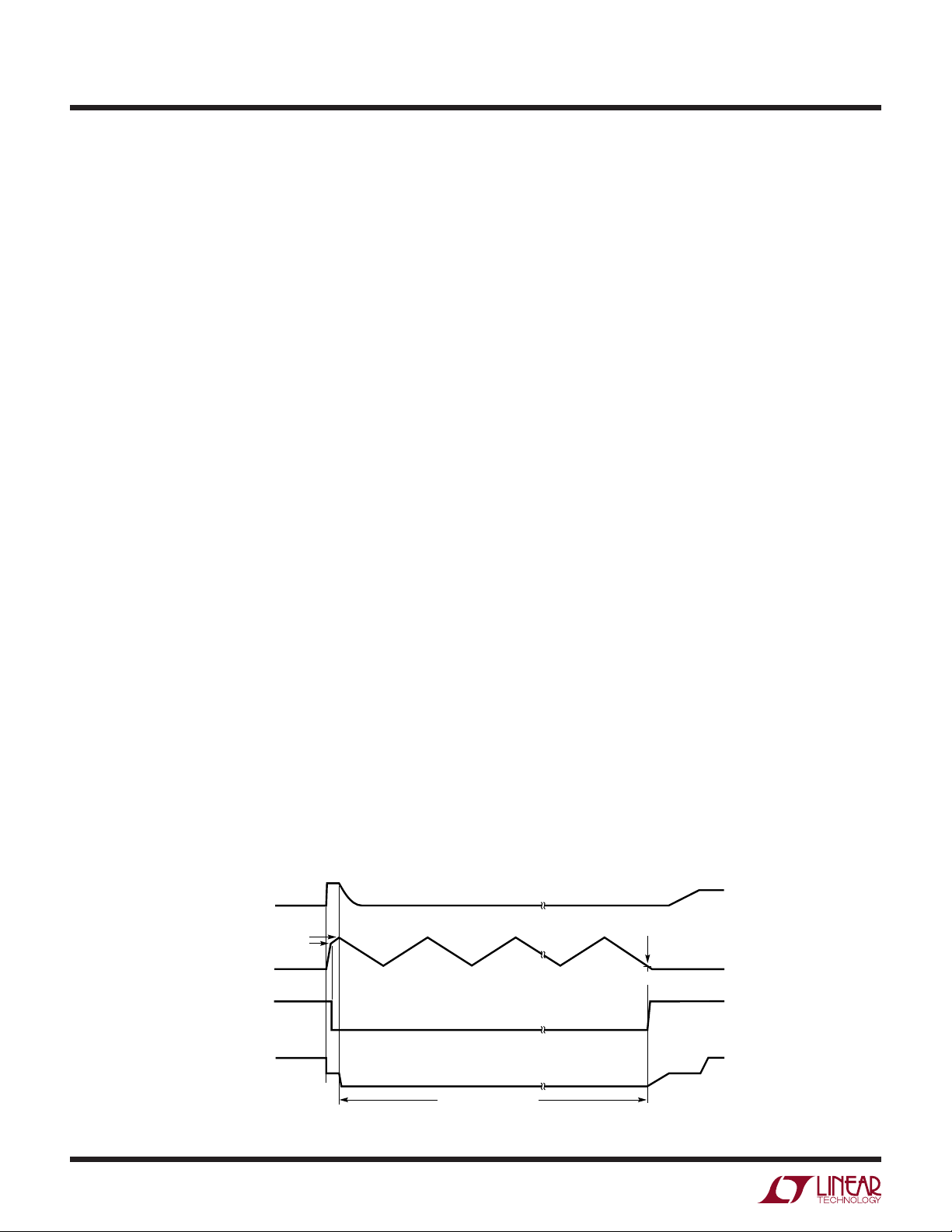
period. If the UV reset pulse is asserted during the cool
down period, the TMR pulses are unaffected and the part
restarts after the cool down period ends. If OV is higher
than 1.25V while UV reset pulse is applied, the part will
not restart until OV drops below 1.25V even if the cool
down period ends.
The second method of restarting the LTC4364-1 is to
pulse the SHDN pin low for more than 200μs. If this is
applied during the cool down period, the cool down timer
is reset with 1mA quickly discharging the TMR pin, and
the part will restart when TMR drops below 0.15V. If the
SHDN reset pulse is applied after the cool down period,
the part restarts immediately. Sufficient cool down time
should be allowed before toggling the SHDN pin to prevent
overstressing the pass device.
A UV reset pulse has no effect on the operation of the
LTC4364-2. However, if a SHDN reset pulse as described
above is asserted in the middle of the cool down period, the
TMR pin quickly discharges with 1mA and the LTC4364-2
is allowed to restart once TMR drops below 0.15V. The OV
pin gates the restart of either LTC4364-1 or LTC4364-2
with a SHDN reset pulse. The part will not restart until OV
drops below 1.25V.
Reverse Input Protection
The LTC4364 can withstand reverse voltage without dam-
age. The V
CC
, SHDN, UV, OV, HGATE, SOURCE and DGATE
pins can all withstand up to –40V with respect to GND.
The LTC4364 controls a second N-channel MOSFET (M2)
as an ideal diode to replace an in-line blocking diode for
reverse input protection with minimum voltage drop in
normal operation. In the event of an input short or a power
supply brownout, reverse current may temporarily flow
through M2. The LTC4364 detects this reverse current
and immediately pulls the DGATE pin to the SOURCE pin,
turning off M2. This minimizes discharge of the output
reservoir capacitor and holds up the output voltage. In
the case where the input supply drops below ground, the
SOURCE pin is pulled below ground through the body
diode of M1. The LTC4364 responds to this condition by
shorting the DGATE pin to the SOURCE pin, keeping M2 off.
MOSFET Selection
The LTC4364 drives two N-channel MOSFETs, M1 and M2,
as the pass devices to conduct the load current (Figure1).
The important features are on-resistance, R
DS(ON)
, the
maximum drain-source voltage, V
(BR)DSS
, the threshold
voltage, and the safe operating area, SOA.
The maximum drain-source voltage rating must be higher
than the maximum input voltage. If the output is shorted to
ground or in an overvoltage event, the full supply voltage
will appear across M1. If the input is shorted to ground,
M2 will be stressed by the voltage held up at the output.
The gate drive for both MOSFETs is guaranteed to be more
than 10V and less than 16V for those applications with V
CC
higher than 8V. This allows the use of standard threshold
voltage N-channel MOSFETs. For systems with V
CC
less
than 8V, a logic-level MOSFET is required since the gate
drive can be as low as 5V. For supplies of 24V or higher, a
15V Zener diode is recommended to be placed between
1.35V
1.25V
FB
TMR
∆V
HGATE
F LT
1.25V
<1.25V
1st 2nd 31st
0.15V
32nd
436412 F04
OV < 1.25V CHECKED
COOL DOWN PERIOD
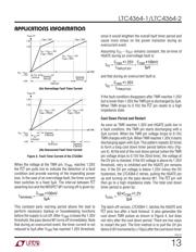
Figure 4. Auto-Retry Cool Down Timer Cycle Following an Overvoltage Fault (LTC4364-2 Only)
APPLICATIONS INFORMATION
器件 Datasheet 文档搜索
AiEMA 数据库涵盖高达 72,405,303 个元件的数据手册,每天更新 5,000 多个 PDF 文件
