Datasheet 搜索 > 电池管理芯片 > Linear Technology(凌力尔特) > LTC4364IDE-2#PBF 数据手册 > LTC4364IDE-2#PBF 数据手册 4/24 页
 器件3D模型
¥ 501.431
LTC4364IDE-2#PBF 数据手册 - Linear Technology(凌力尔特)
制造商:
Linear Technology(凌力尔特)
分类:
电池管理芯片
封装:
DFN-14
描述:
LINEAR TECHNOLOGY LTC4364IDE-2#PBF 芯片, 电涌消除器, 4/80V, 自动重试, 14DFN
Pictures:
3D模型
符号图
焊盘图
引脚图
产品图
页面导航:
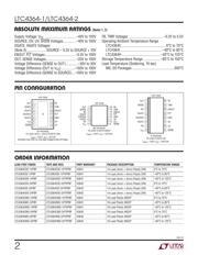
引脚图在P7P8Hot
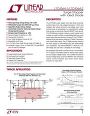
典型应用电路图在P1P19P20P21P24
原理图在P9
封装尺寸在P21
焊盘布局在P22P23
型号编码规则在P3
标记信息在P3
封装信息在P3
技术参数、封装参数在P4
应用领域在P1P7P8P11P12P13P14P15P16P17P18P19
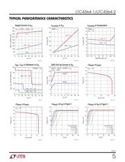
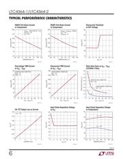
电气规格在P3P4P5P6P12

导航目录
LTC4364IDE-2#PBF数据手册
Page:
of 24 Go
若手册格式错乱,请下载阅览PDF原文件
LTC4364-1/LTC4364-2
4
436412f
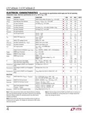
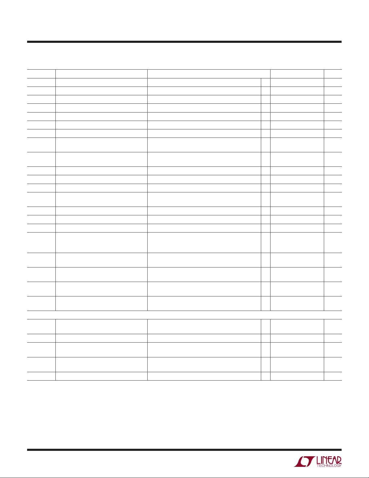
ELECTRICAL CHARACTERISTICS
The l denotes the specifications which apply over the full operating
temperature range, otherwise specifications are at T
A
= 25°C. V
CC
= 12V.
SYMBOL PARAMETER CONDITIONS MIN TYP MAX UNITS
V
TMR(R)
TMR Retry Threshold HGATE Rising (After 32 Cycles), V
CC
= 4V to 80V
l
0.125 0.15 0.175 V
∆V
TMR
Early Warning Timer Window V
TMR(G)
– V
TMR(F)
, V
CC
= 4V to 80V
l
75 100 125 mV
V
UV
UV Input Threshold UV Falling, V
CC
= 4V to 80V
l
1.22 1.25 1.28 V
V
UV(HYST)
UV Input Hysteresis
l
25 50 80 mV
V
UV(RST)
UV Reset Threshold UV Falling, V
CC
= 4V to 80V, LTC4364-1 Only
l
0.5 0.6 0.7 V
V
OV
OV Input Threshold OV Rising, V
CC
= 4V to 80V
l
1.22 1.25 1.28 V
V
OV(HYST)
OV Input Hysteresis 12 mV
I
IN
UV, OV Input Current UV, OV = 1.25V
UV, OV = –30V
l
l
0
–0.3
1
–0.6
µA
mA
V
OL
ENOUT, F LT Output Low I
SINK
= 0.25mA
I
SINK
= 2mA
l
l
0.1
0.5
0.3
1.3
V
V
I
LEAK
ENOUT, F LT Leakage Current ENOUT, F LT = 80V
l
0 2.5 µA
∆V
OUT(TH)
Out High Threshold (V
CC
– V
OUT
) ENOUT from Low to High
l
0.4 0.7 1 V
V
OUT(RST)
Out Reset Threshold ENOUT from High to Low
l
1.4 2.2 3 V
I
OUT
OUT Input Current V
CC
= OUT = 12V, SHDN Open
OUT = –15V
l
l
40
–4
80
–8
µA
mA
Output Current in Shutdown, I
SNS
+ I
OUT
V
CC
= SOURCE = SENSE = OUT = 12V, Shutdown
l
12 40 µA
V
SHDN
SHDN Input Threshold V
CC
= 4V to 80V
l
0.5 1.6 2.2 V
V
SHDN(FLT)
SHDN Pin Float Voltage V
CC
= 12V to 80V
l
2.3 4 6.5 V
I
SHDN
SHDN Input Current SHDN = 0.5V
Maximum Allowable Leakage, V
CC
= 4V
SHDN = –30V
l
l
–1 –3.3
–1.5
–120
–300
µA
µA
µA
D Retry Duty Cycle, Overvoltage
Retry Duty Cycle, Output Short
FB = 1.5V, V
CC
= 80V, OUT = 16V
∆V
SNS
= 60mV, V
CC
– OUT = 12V
l
l
0.125
0.075
0.2
0.12
%
%
t
OFF,HGATE(UV)
Undervoltage to HGATE Low Propagation
Delay
UV Steps from 1.5V to 1V
l
1.3 4 μs
t
OFF,HGATE(OV)
Overvoltage to HGATE Low Propagation
Delay
FB Steps from 1V to 1.5V
l
0.25 1 μs
t
OFF,HGATE(OC)
Overcurrent to HGATE Low Propagation
Delay
∆V
SNS
Steps from 0mV to 150mV, OUT = 0V
l
0.5 2 μs
Ideal Diode
ΔV
DGATE
DGATE Gate Drive, (V
DGATE
− V
SOURCE
) V
CC
= 4V, No Fault, I
DGATE
= 0µA, −1µA
V
CC
= 8V to 80V, No Fault, I
DGATE
= 0µA, −1µA
l
l
5
10
8.5
12
12
16
V
V
I
DGATE(UP)
DGATE Pin Pull-Up Current
DGATE = SOURCE = V
CC
= 12V, ∆V
SD
= 0.1V
l
–5 –10 –15 µA
I
DGATE(DN)
DGATE Pin Pull-Down Current
∆V
DGATE
= 5V, ∆V
SD
= –0.2V
∆V
DGATE
= 5V, Shutdown/Fault Turn-Off
l
l
60
0.4
130
1
mA
mA
∆V
SD
Ideal Diode Regulation Voltage,
(V
SOURCE
− V
SENSE
)
∆V
DGATE
= 2.5V, V
CC
= SOURCE = 12V
∆V
DGATE
= 2.5V, V
CC
= SOURCE = 4V
l
l
10
24
30
48
45
72
mV
mV
t
OFF(DGATE)
DGATE Turn-Off Propagation Delay
∆V
SD
Steps from 0.1V to –1V
l
0.35 1.5 μs
Note 1: Stress beyond those listed under Absolute Maximum Ratings
may cause permanent damage to the device. Exposure to any Absolute
Maximum Rating condition for extended periods may affect device
reliability and lifetime.
Note 2: All Currents into device pins are positive and all currents out
of device pins are negative. All voltages are referenced to GND unless
otherwise specified.
Note 3: Internal clamps limit the HGATE and DGATE pins to minimum of
10V above the SOURCE pin. Driving these pins to voltages beyond the
clamp may damage the device.
器件 Datasheet 文档搜索
AiEMA 数据库涵盖高达 72,405,303 个元件的数据手册,每天更新 5,000 多个 PDF 文件
