Datasheet 搜索 > Modern Technology > M29W128GH70ZS6E 数据手册 > M29W128GH70ZS6E 数据手册 5/77 页


¥ 12.138
M29W128GH70ZS6E 数据手册 - Modern Technology
制造商:
Modern Technology
Pictures:
3D模型
符号图
焊盘图
引脚图
产品图
页面导航:

导航目录
M29W128GH70ZS6E数据手册
Page:
of 77 Go
若手册格式错乱,请下载阅览PDF原文件

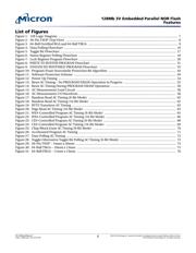
List of Figures
Figure 1: 128 Logic Diagram ............................................................................................................................ 7
Figure 2: 56-Pin TSOP (Top View) .................................................................................................................... 8
Figure 3: 64-Ball Fortified BGA and 64-Ball TBGA ............................................................................................. 9
Figure 4: Data Polling Flowchart .................................................................................................................... 16
Figure 5: Toggle Bit Flowchart ........................................................................................................................ 17
Figure 6: Status Register Polling Flowchart ..................................................................................................... 18
Figure 7: Lock Register Program Flowchart ..................................................................................................... 20
Figure 8: WRITE TO BUFFER PROGRAM Flowchart ........................................................................................ 31
Figure 9: ENHANCED BUFFERED PROGRAM Flowchart ................................................................................ 35
Figure 10: Program/Erase Nonvolatile Protection Bit Algorithm ...................................................................... 44
Figure 11: Software Protection Scheme .......................................................................................................... 49
Figure 12: Power-Up Timing .......................................................................................................................... 54
Figure 13: Reset AC Timing – No PROGRAM/ERASE Operation in Progress ...................................................... 55
Figure 14: Reset AC Timing During PROGRAM/ERASE Operation .................................................................... 56
Figure 15: AC Measurement Load Circuit ....................................................................................................... 58
Figure 16: AC Measurement I/O Waveform ..................................................................................................... 58
Figure 17: Random Read AC Timing (8-Bit Mode) ........................................................................................... 62
Figure 18: Random Read AC Timing (16-Bit Mode) ......................................................................................... 62
Figure 19: BYTE Transition AC Timing ............................................................................................................ 63
Figure 20: Page Read AC Timing (16-Bit Mode) ............................................................................................... 63
Figure 21: WE#-Controlled Program AC Timing (8-Bit Mode) .......................................................................... 65
Figure 22: WE#-Controlled Program AC Timing (16-Bit Mode) ......................................................................... 66
Figure 23: CE#-Controlled Program AC Timing (8-Bit Mode) ........................................................................... 68
Figure 24: CE#-Controlled Program AC Timing (16-Bit Mode) ......................................................................... 69
Figure 25: Chip/Block Erase AC Timing (8-Bit Mode) ...................................................................................... 70
Figure 26: Accelerated Program AC Timing ..................................................................................................... 71
Figure 27: Data Polling AC Timing .................................................................................................................. 72
Figure 28: Toggle/Alternative Toggle Bit Polling AC Timing (8-Bit Mode) .......................................................... 72
Figure 29: 56-Pin TSOP – 14mm x 20mm ........................................................................................................ 74
Figure 30: 64-Ball TBGA – 10mm x 13mm ....................................................................................................... 75
Figure 31: 64-Ball FBGA – 11mm x 13mm ....................................................................................................... 76
128Mb 3V Embedded Parallel NOR Flash
Features
PDF: 09005aef84daa141
m29w_128mb.pdf - Rev. B 5/15 EN
5
Micron Technology, Inc. reserves the right to change products or specifications without notice.
© 2012 Micron Technology, Inc. All rights reserved.
器件 Datasheet 文档搜索
AiEMA 数据库涵盖高达 72,405,303 个元件的数据手册,每天更新 5,000 多个 PDF 文件
