Datasheet 搜索 > 多工器 > Maxim Integrated(美信) > MAX14803CCM+CP3 数据手册 > MAX14803CCM+CP3 数据手册 2/20 页
 器件3D模型
¥ 339.07
MAX14803CCM+CP3 数据手册 - Maxim Integrated(美信)
制造商:
Maxim Integrated(美信)
分类:
多工器
封装:
LQFP
Pictures:
3D模型
符号图
焊盘图
引脚图
产品图
页面导航:
导航目录
MAX14803CCM+CP3数据手册
Page:
of 20 Go
若手册格式错乱,请下载阅览PDF原文件
MAX14802/MAX14803/MAX14803A
Low-Charge Injection, 16-Channel,
High-Voltage Analog Switches
2
Maxim Integrated
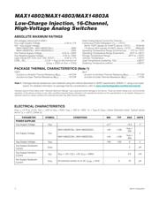
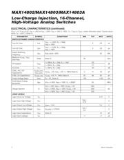
ABSOLUTE MAXIMUM RATINGS
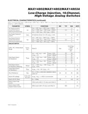
ELECTRICAL CHARACTERISTICS
(V
DD
= +2.7V to +5.5V, V
PP
= +40V to V
NN
+ 250V, V
NN
= -40V to -160V, T
A
= T
MIN
to T
MAX
, unless otherwise noted. Typical values
are at T
A
= +25°C.) (Note 2)
Stresses beyond those listed under “Absolute Maximum Ratings” may cause permanent damage to the device. These are stress ratings only, and functional
operation of the device at these or any other conditions beyond those indicated in the operational sections of the specifications is not implied. Exposure to
absolute maximum rating conditions for extended periods may affect device reliability.
Note 1: Package thermal resistances were obtained using the method described in JEDEC specification JESD51-7, using a four-layer
board. For detailed information on package thermal considerations, refer to www.maximintegrated.com/thermal-tutorial
.
(All voltages referenced to GND.)
V
DD
Logic-Supply Voltage .......................................-0.3V to +7V
V
PP
- V
NN
Supply Voltage
(MAX14802CCM+, MAX14803CCM+)..............................260V
(MAX14802ECM+, MAX14803AEWZ+) ............................230V
V
PP
Positive-Supply Voltage.................................-0.3V to +220V
V
NN
Negative-Supply Voltage ...............................-0.3V to -220V
Logic Inputs (LE, CLR, CLK, DIN, DOUT)................-0.3V to +7V
COM_, NO_...............................(-0.3V + V
NN
) to the minimum of
[(V
NN
+ 220V) or (V
PP
+ 0.3V)]
Peak Analog Signal Current Per Channel ................................3A
Continuous Power Dissipation (T
A
= +70°C)
48-Pin TQFP (derate 22.7mW/°C above +70°C).........1818mW
110-Bump WLP (derate 37mW°C above +70°C)........2960mW
Operating Temperature Range (Commercial)........0°C to +70°C
Operating Temperature Range (Extended).........-40°C to +85°C
Storage Temperature Range .............................-65°C to +150°C
Junction Temperature..................................................... +150°C
Lead Temperature (soldering, 10s) .................................+300°C
Soldering Temperature (reflow) .......................................+260°C
PACKAGE THERMAL CHARACTERISTICS (Note 1)
TQFP
Junction-to-Ambient Thermal Reistance (
θ
JA
)..............44°C/W
Junction-to-Case Thermal Resistance (
θ
JC
).................10°C/W
WLP
Junction-to-Ambient Thermal Reistance (
θ
JA
)..............27°C/W
Junction-to-Case Thermal Resistance (
θ
JC
)...................1°C/W
PARAMETER SYMBOL CONDITIONS MIN TYP MAX UNITS
POWER SUPPLIES
V
DD
Supply Voltage V
DD
+2.7 +5.5 V
MAX14802ECM+, MAX14803AEWZ+ +40 +100
V
NN
+
200
V
PP
Supply Voltage V
PP
MAX14802CCM+, MAX14803CCM+ +40 +100
V
NN
+
250
V
V
NN
Supply Voltage V
NN
-160 -100 0 V
V
DD
Supply Quiescent
Current
I
DDQ
5μA
V
DD
Supply Dynamic
Current
I
DD
V
DD
= +5V, V
LE
= +5V, f
CLK
= 5MHz 0.5 mA
V
PP
Supply Quiescent
Current
I
PPQ
All switches remain on or off, I
COM_
= 5mA 0 10 μA
器件 Datasheet 文档搜索
AiEMA 数据库涵盖高达 72,405,303 个元件的数据手册,每天更新 5,000 多个 PDF 文件
