Datasheet 搜索 > 多工器 > Maxim Integrated(美信) > MAX14803CCM+CP3 数据手册 > MAX14803CCM+CP3 数据手册 5/20 页
 器件3D模型
¥ 339.07
MAX14803CCM+CP3 数据手册 - Maxim Integrated(美信)
制造商:
Maxim Integrated(美信)
分类:
多工器
封装:
LQFP
Pictures:
3D模型
符号图
焊盘图
引脚图
产品图
页面导航:
导航目录
MAX14803CCM+CP3数据手册
Page:
of 20 Go
若手册格式错乱,请下载阅览PDF原文件
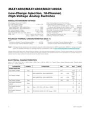
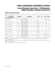
MAX14802/MAX14803/MAX14803A
Low-Charge Injection, 16-Channel,
High-Voltage Analog Switches
5
Maxim Integrated
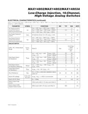
TIMING CHARACTERISTICS
(V
DD
= +2.7V to +5.5V, V
PP
= +40V to V
NN
+ 200V, V
NN
= -40V to -160V, T
A
= T
MIN
to T
MAX
, unless otherwise noted. Typical values
are at T
A
= +25°C.) (Note 2)
PARAMETER SYMBOL CONDITIONS MIN TYP MAX UNITS
LOGIC TIMING (Figure 1)
V
DD
= +5V ±10% 20
CLK Frequency f
CLK
V
DD
= +3V ±10% 10
MHz
V
DD
= +5V ±10% 10
DIN to CLK Setup Time t
DS
V
DD
= +3V ±10% 16
ns
V
DD
= +5V ±10% 3
DIN to CLK Hold Time t
DH
V
DD
= +3V ±10% 3
ns
V
DD
= +5V ±10% 36
CLK to LE Setup Time t
CS
V
DD
= +3V ±10% 65
ns
V
DD
= +5V ±10% 14
LE Low-Pulse Width t
WL
V
DD
= +3V ±10% 22
ns
V
DD
= +5V ±10% 20
CLR High-Pulse Width t
WC
V
DD
= +3V ±10% 40
ns
V
DD
= +5V ±10% 50
CLK Rise and Fall Times t
R
, t
F
V
DD
= +3V ±10% 50
ns
V
DD
= +5V ±10% 6 42
CLK to DOUT Delay t
DO
V
DD
= +3V ±10% 12 80
ns
Note 2: All devices are 100% tested at T
A
= +70°C. Limits over the operating temperature range are guaranteed by design and
characterization.
Note 3: The analog signal input V
COM_
and V
NO_
must satisfy V
NN
≤ (V
COM_
, V
NO_
) ≤ V
PP
, or remain unconnected during power-up
and power-down.
Note 4: Guaranteed by characterization; not production tested.
器件 Datasheet 文档搜索
AiEMA 数据库涵盖高达 72,405,303 个元件的数据手册,每天更新 5,000 多个 PDF 文件
