Datasheet 搜索 > 接口隔离器 > Maxim Integrated(美信) > MAX14850AEE+T 数据手册 > MAX14850AEE+T 数据手册 2/17 页
 器件3D模型
¥ 15.521
MAX14850AEE+T 数据手册 - Maxim Integrated(美信)
制造商:
Maxim Integrated(美信)
分类:
接口隔离器
封装:
SSOP-16
描述:
数字隔离器 Six Channel 600vrms Digital Isolator
Pictures:
3D模型
符号图
焊盘图
引脚图
产品图
页面导航:
引脚图在P11P12Hot
典型应用电路图在P1P12P15P16
封装尺寸在P16
型号编码规则在P1P16
封装信息在P16
功能描述在P1
技术参数、封装参数在P6
应用领域在P1P14
电气规格在P3P4P5P13
导航目录
MAX14850AEE+T数据手册
Page:
of 17 Go
若手册格式错乱,请下载阅览PDF原文件
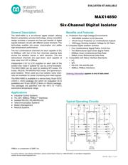
MAX14850
Six-Channel Digital Isolator
2Maxim Integrated
V
CCA
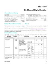
to GNDA ........................................................-0.3V to +6V
V
CCB
to GNDB ........................................................-0.3V to +6V
OUTA1, OUTA2 to GNDA ..................... -0.3V to (V
CCA
+ 0.3V)
OUTB1, OUTB2 to GNDB ..................... -0.3V to (V
CCB
+ 0.3V)
INB1, INB2, I/OA1, I/OA2 to GNDA ........................-0.3V to +6V
INA1, INA2, I/OB1, I/OB2 to GNDB ........................-0.3V to +6V
Short-Circuit Duration (OUTA_ to GNDA or
V
CCA
, OUTB_ to GNDB or V
CCB
) .........................Continuous
Continuous Current (I/OA_, I/OB_) Pin ............................ Q50mA
Continuous Power Dissipation (T
A
= +70NC)
SOIC (derate 13.3mW/NC above +70NC) ..............1067mW
QSOP (derate 9.6mW/NC above +70NC)..............771.5mW
Operating Temperature Range ........................ -40NC to +125NC
Junction Temperature .....................................................+150NC
Storage Temperature Range ............................ -65NC to +150NC
Lead Temperature (soldering, 10s) ................................+300NC
Soldering Temperature (reflow) ......................................+260NC
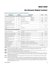
Absolute Maximum Ratings
Note 1: Package thermal resistances were obtained using the method described in JEDEC specification JESD51-7, using a four-layer
board. For detailed information on package thermal considerations, refer to www.maximintegrated.com/thermal-tutorial.
Stresses beyond those listed under “Absolute Maximum Ratings” may cause permanent damage to the device. These are stress ratings only, and functional operation
of the device at these or any other conditions beyond those indicated in the operational sections of the specifications is not implied. Exposure to absolute maximum
rating conditions for extended periods may affect device reliability.
SOIC
Junction-to-Ambient Thermal Resistance (B
JA
) ..........75NC/W
Junction-to-Case Thermal Resistance (B
JC
) ...............24NC/W
QSOP
Junction-to-Ambient Thermal Resistance (B
JA
) .....103.7NC/W
Junction-to-Case Thermal Resistance (B
JC
) ...............37NC/W
Package Thermal Characteristics
(Note 1)
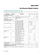
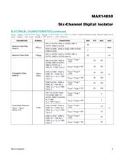
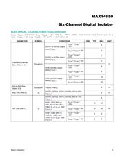
Electrical Characteristics
(V
CCA
- V
GNDA
= 3.0V to 5.5V, V
CCB
- V
GNDB
= 3.0V to 5.5V, T
A
= -40°C to +125°C, unless otherwise noted. Typical values are at
V
CCA
- V
GNDA
= 3.3V, V
CCB
- V
GNDB
= 3.3V, and T
A
= +25°C.) (Note 2)
PARAMETER SYMBOL CONDITIONS MIN TYP MAX UNIT
DC CHARACTERISTICS
Supply Voltage
V
CCA
Relative to GNDA 3.0 5.5
V
V
CCB
Relative to GNDB 3.0 5.5
Supply Current
I
CCA
,
I
CCB
Unidirectional inputs
at DC or 2Mbps;
bidirectional inputs at DC
or switching at 2Mbps,
no load
V
CCA
= +5V,
V
CCB
= +5V
7.2 11
mA
V
CCA
= +3.3V,
V
CCB
= +3.3V
6.2 9.5
All inputs switching at
max data rate. No load.
(Note 3)
V
CCA
= +5V,
V
CCB
=
+5V
T
A
=
+25°C
15 22
T
A
=
+125°C
17 24
V
CCA
=
+3.3V,
V
CCB
=
+3.3V
T
A
=
+25°C
10 16
T
A
=
+125°C
11 18
Undervoltage-Lockout
Threshold
V
UVLO
V
CCA
- V
GNDA
, V
CCB
- V
GNDB
(Note 4) 2 V
Undervoltage-Lockout
Hysteresis
V
UVLOHYS
V
CCA
- V
GNDA
, V
CCB
- V
GNDB
(Note 4) 0.1 V
器件 Datasheet 文档搜索
AiEMA 数据库涵盖高达 72,405,303 个元件的数据手册,每天更新 5,000 多个 PDF 文件
