Datasheet 搜索 > 稳压芯片 > Maxim Integrated(美信) > MAX1904ETJ+T 数据手册 > MAX1904ETJ+T 数据手册 4/33 页
 器件3D模型
¥ 71.477
MAX1904ETJ+T 数据手册 - Maxim Integrated(美信)
制造商:
Maxim Integrated(美信)
分类:
稳压芯片
封装:
TQFN-32
Pictures:
3D模型
符号图
焊盘图
引脚图
产品图
页面导航:
引脚图在P1P9P10P30Hot
典型应用电路图在P1P14P24
原理图在P15P16
封装尺寸在P31P32P33
型号编码规则在P1
功能描述在P1
技术参数、封装参数在P6
应用领域在P1P20P24
电气规格在P3P4P5P6P21P23P24
导航目录
MAX1904ETJ+T数据手册
Page:
of 33 Go
若手册格式错乱,请下载阅览PDF原文件
MAX1901/MAX1902/MAX1904
500kHz Multi-Output, Low-Noise Power-Supply
Controllers for Notebook Computers
4 _______________________________________________________________________________________
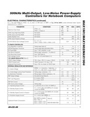
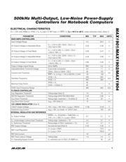
ELECTRICAL CHARACTERISTICS (continued)
(V+ = 15V, both PWMs on, SYNC = V
L
, V
L
load = 0, REF load = 0, SKIP = 0, T
A
= 0°C to +85°C, unless otherwise noted. Typical
values are at T
A
= +25°C.)
PARAMETER CONDITIONS MIN TYP MAX UNITS
FAULT DETECTION (MAX1901/MAX1902)
Overvoltage Trip Threshold With respect to unloaded output voltage 4 7 10 %
Overvoltage Fault Propagation Delay
CSL_ driven 2% above overvoltage trip
threshold
1.5 µs
Output Undervoltage Threshold With respect to unloaded output voltage 60 70 80 %
Output Undervoltage Lockout Time
From each SMPS enabled, with respect to
f
OSC
5,000 6,144 7,000 clks
Thermal-Shutdown Threshold Typical hysteresis = 10°C 150 °C
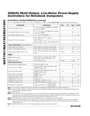
RESET
RESET Trip Threshold
With respect to unloaded output voltage,
falling edge; typical hysteresis = 1%
-7 -5.5 -4 %
RESET Propagation Delay
Falling edge, CSL_ driven 2% below RESET
trip threshold
1.5 µs
RESET Delay Time With respect to f
OSC
27,000 32,000 37,000 clks
INPUTS AND OUTPUTS
Feedback-Input Leakage Current FB3, FB5; SECFB = 2.6V 1 50 nA
Logic Input-Low Voltage
RUN/ON3, SKIP, TIME/ON5 (SEQ = REF),
SHDN, STEER, SYNC
0.6 V
Logic Input-High Voltage
RUN/ON3, SKIP, TIME/ON5 (SEQ = REF),
SHDN, STEER, SYNC
2.4 V
Input Leakage Current
RUN/ON3, SKIP, TIME/ON5 (SEQ = REF),
SHDN, STEER, SYNC, SEQ; V
PIN
= 0V or 3.3V
±1µA
Logic Output-Low Voltage RESET, I
SINK
= 4mA 0.4 V
Logic Output-High Current RESET = 3.5V 1 mA
TIME/ON5 Input Trip Level SEQ = 0 or V
L
2.4 2.6 V
TIME/ON5 Source Current TIME/ON5 = 0, SEQ = 0 or V
L
2.5 3 3.5 µA
TIME/ON5 On-Resistance TIME/ON5; RUN/ON3 = 0, SEQ = 0 or V
L
15 80 Ω
Gate-Driver Sink/Source Current DL3, DH3, DL5, DH5; forced to 2V 1 A
SSOP package 1.5 7
Gate-Driver On-Resistance High or low (Note 6)
QFN package 1.5 8
Ω
器件 Datasheet 文档搜索
AiEMA 数据库涵盖高达 72,405,303 个元件的数据手册,每天更新 5,000 多个 PDF 文件
