Datasheet 搜索 > 主动器件 > Maxim Integrated(美信) > MAX3815CCM+D 数据手册 > MAX3815CCM+D 数据手册 6/11 页
 器件3D模型
¥ 133.289
MAX3815CCM+D 数据手册 - Maxim Integrated(美信)
制造商:
Maxim Integrated(美信)
分类:
主动器件
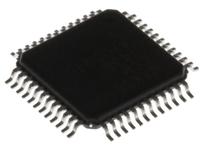
封装:
TQFP-48
描述:
Maxim Integrated### 视频,Maxim Integrated
Pictures:
3D模型
符号图
焊盘图
引脚图
产品图
页面导航:
导航目录
MAX3815CCM+D数据手册
Page:
of 11 Go
若手册格式错乱,请下载阅览PDF原文件
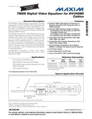
MAX3815
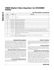
Detailed Description
The MAX3815 TMDS equalizer accepts differential CML
input data at rates of 250Mbps up to 1.65Gbps (individ-
ual channel data rate). It automatically adjusts to atten-
uation levels of up to 40dB at 825MHz due to
skin-effect losses in copper cable. It consists of four
CML input buffers, a loss-of-clock signal detector, three
independent adaptive equalizers, four limiting ampli-
fiers, and four output buffers (Figure 1).
CML Input Buffers and Output Drivers
The input buffers and the output drivers are implement-
ed using current-mode logic (CML) (see Figures 3 and
4). The output drivers are open-collector and can be
turned off with the OUTON pin, or can be set to output
a one-half amplitude signal (500mV
P-P
differential)
using the OUTLEVEL pin. For details on interfacing with
CML, refer to Maxim Application Note
HFAN-01.0:
Introduction to LVDS, PECL, and CML
.
Loss-of-Clock Signal Detector
The loss-of-clock signal detector indicates a loss-of-
clock signal at the CLKLOS pin.
Adaptive Equalizer
The three data channels each contain an independent
adaptive equalizer. Each channel analyzes the incom-
ing signal and determines the amount of equalization to
apply.
Limiting Amplifier
The limiting amplifier amplifies the signal from the
adaptive equalizer and truncates the top and bottom of
the waveform to provide a clean high- and low-level
signal to the output drivers.
Applications Information
Typical shielded twisted pair (STP) and unshielded
twisted pair (UTP) cables exhibit skin-effect losses,
which attenuate the high-frequency spectrum of a
TMDS signal, eventually causing data errors or even
closing the signal eye altogether given a long enough
cable. The MAX3815 recovers the data and opens the
signal eye through compensating equalization.
The basic TMDS interface is composed of four differen-
tial serial links: three links carry serial data up to
1.65Gbps each, and the fourth is a one-tenth-rate
(0.1x) clock that operates up to 165MHz. TMDS, as with
TMDS Digital Video Equalizer for DVI/HDMI
Cables
6 _______________________________________________________________________________________
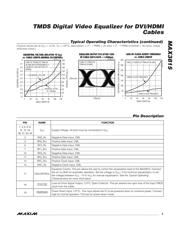
Pin Description (continued)
PIN NAME FUNCTION
20, 23, 24,
25, 28, 29,
32, 33, 36,
37, 42
GND Ground
21 RXC_OUT- Negative Clock Output, CML
22 RXC_OUT+ Positive Clock Output, CML
26 RX2_OUT+ Positive Data Output, CML
27 RX2_OUT- Negative Data Output, CML
30 RX1_OUT+ Positive Data Output, CML
31 RX1_OUT- Negative Data Output, CML
34 RX0_OUT+ Positive Data Output, CML
35 RX0_OUT- Negative Data Output, CML
39 OUTLEVEL
Output-Level Control Input, LVTTL. This input sets the output amplitude to the standard DVI level
(1000mV
P-P
) when high, and sets the output amplitude to 1/2 the DVI level (500mV
P-P
) when low.
40 OUTON
Output-Enable Control Input, LVTTL. This input enables the CML outputs when forced low and sets a
differential logic zero when forced high.
45–48 N.C. No Connection
EP Exposed Pad
Ground. The exposed pad must be soldered to the circuit-board ground for proper
thermal and electrical operation.
器件 Datasheet 文档搜索
AiEMA 数据库涵盖高达 72,405,303 个元件的数据手册,每天更新 5,000 多个 PDF 文件
