Datasheet 搜索 > 接口芯片 > Maxim Integrated(美信) > MAX7311AUG+ 数据手册 > MAX7311AUG+ 数据手册 2/16 页
 器件3D模型
¥ 69.697
MAX7311AUG+ 数据手册 - Maxim Integrated(美信)
制造商:
Maxim Integrated(美信)
分类:
接口芯片
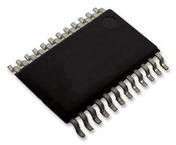
封装:
TSSOP-24
描述:
MAXIM INTEGRATED PRODUCTS MAX7311AUG+ 输入/输出扩展, 16bit, 400 kHz, I2C, 2 V, 5.5 V, TSSOP
Pictures:
3D模型
符号图
焊盘图
引脚图
产品图
页面导航:
导航目录
MAX7311AUG+数据手册
Page:
of 16 Go
若手册格式错乱,请下载阅览PDF原文件
MAX7311
2-Wire-Interfaced 16-Bit I/O Port Expander
with Interrupt and Hot-Insertion Protection
2 _______________________________________________________________________________________
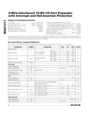
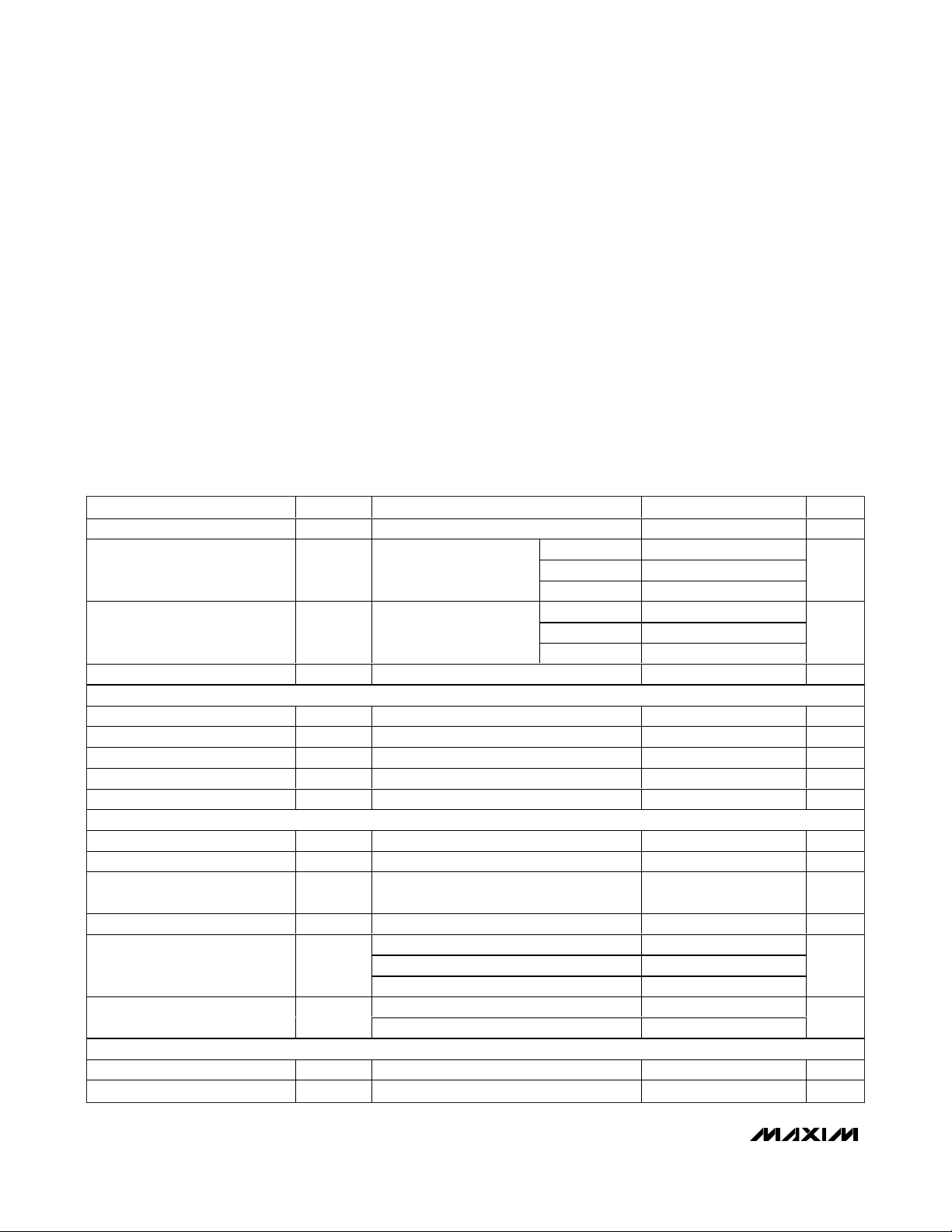
ABSOLUTE MAXIMUM RATINGS
DC ELECTRICAL CHARACTERISTICS
(V
+
= 2V to 5.5V, T
A
= -40°C to +125°C, unless otherwise noted. Typical values are at V
+
= 3.3V, T
A
= +25°C.) (Note 1)
Stresses beyond those listed under “Absolute Maximum Ratings” may cause permanent damage to the device. These are stress ratings only, and functional
operation of the device at these or any other conditions beyond those indicated in the operational sections of the specifications is not implied. Exposure to
absolute maximum rating conditions for extended periods may affect device reliability.
V
+
to GND ................................................................-0.3V to +6V
I/O0–I/O15 as Inputs ....................................(GND - 0.3V) to +6V
SCL, SDA, AD0, AD1, AD2, INT...................(GND - 0.3V) to +6V
Maximum V
+
Current ......................................................+250mA
Maximum GND Current ...................................................-250mA
DC Input Current on I/O0–I/O15 .......................................±20mA
DC Output Current on I/O0–I/O15 ....................................±80mA
Continuous Power Dissipation (T
A
= +70°C)
24-Pin Wide SO (derate 11.8mW/°C above +70°C) ....941mW
24-Pin SSOP (derate 8.0mW/°C above +70°C) ...........640mW
24-Pin TSSOP (derate 12.2mW/°C above +70°C) .......975mW
24-Pin Thin QFN (derate 20.8mW/°C above +70°C) .1668mW
Operating Temperature Range .........................-40°C to +125°C
Junction Temperature......................................................+150°C
Storage Temperature Range .............................-65°C to +150°C
Lead Temperature (soldering, 10s) .................................+300°C
PARAMETER SYM B O L CONDITIONS MIN TYP MAX UNITS
Supply Voltage V
+
2 5.5 V
V
+
= 2V 23 35
V
+
= 3.3V 43 60Supply Current I
+
All I/Os unloaded,
f
SCL
= 400kHz
V
+
= 5.5V 80 120
µA
V
+
= 2V 2.3 11
V
+
= 3.3V 2.9 12Standby Current I
STBY
All I/Os unloaded,
f
SCL
= 0
V
+
= 5.5V 3.8 15.5
µA
Power-On Reset Voltage V
POR
1.4 1.7 V
SCL, SDA
Input Voltage Low V
IL
0.3 ✕ V
+
V
Input Voltage High
V
IH
0.7 ✕ V
+
V
Low-Level Output Voltage V
OL
I
SINK
= 6mA 0.4 V
Leakage Current I
L
-1 +1 µA
Input Capacitance 10 pF
I/O_
Input Voltage Low V
IL
0.8 V
Input Voltage High V
IH
1.8 V
Input Leakage Current
T
A
= -40°C to +85°C; includes internal
pullup current, V
IO
= V
+
1µA
Internal Pullup Current T
A
= -40°C to +85°C, V
IO
= 0 34 100 µA
V
+
= 2V, V
OL
= 0.5V 8.5 17
V
+
= 3.3V, V
OL
= 0.5V 17 32
Low-Level Output Current I
SINK
V
+
= 5V, V
OL
= 0.5V 43
mA
V
+
= 3.3V, V
OH
= 2.4V 29 41
High Output Current I
SOURCE
V
+
= 5V, V
OH
= 4.5V 31
mA
AD0, AD1, AD2
Input Voltage Low V
IL
0.3 ✕ V
+
V
Input Voltage High V
IH
0.7 ✕ V
+
V
器件 Datasheet 文档搜索
AiEMA 数据库涵盖高达 72,405,303 个元件的数据手册,每天更新 5,000 多个 PDF 文件
