Datasheet 搜索 > 接口芯片 > Maxim Integrated(美信) > MAX7311AUG+ 数据手册 > MAX7311AUG+ 数据手册 3/16 页
 器件3D模型
¥ 69.697
MAX7311AUG+ 数据手册 - Maxim Integrated(美信)
制造商:
Maxim Integrated(美信)
分类:
接口芯片
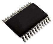
封装:
TSSOP-24
描述:
MAXIM INTEGRATED PRODUCTS MAX7311AUG+ 输入/输出扩展, 16bit, 400 kHz, I2C, 2 V, 5.5 V, TSSOP
Pictures:
3D模型
符号图
焊盘图
引脚图
产品图
页面导航:
导航目录
MAX7311AUG+数据手册
Page:
of 16 Go
若手册格式错乱,请下载阅览PDF原文件
MAX7311
2-Wire-Interfaced 16-Bit I/O Port Expander
with Interrupt and Hot-Insertion Protection
_______________________________________________________________________________________ 3
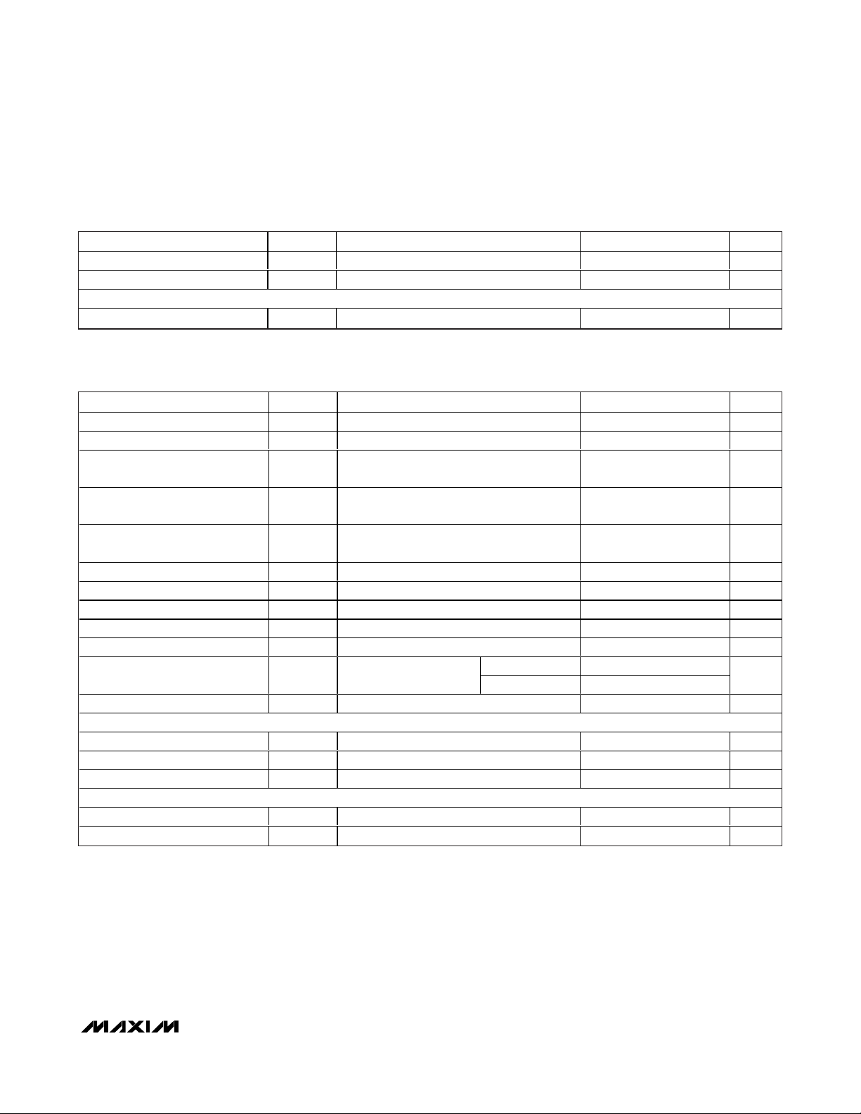
Note 1: All parameters are 100% production tested at T
A
= +25°C. Specifications over temperature are guaranteed by design.
Note 2: Minimum SCL clock frequency is limited by the MAX7311 bus timeout feature, which resets the serial bus interface if either
SDA or SCL is held low for a minimum of 25ms. Disable bus timeout feature for DC operation.
Note 3: A master device must internally provide a hold time of at least 300ns for the SDA signal (referred to the V
IL
of the SCL
signal) in order to bridge the undefined region SCL’s falling edge.
Note 4: C
B
= total capacitance of one bus line in pF.
Note 5: The maximum t
F
for the SDA and SCL bus lines is specified at 300ns. The maximum fall time for the SDA output stage t
F
is
specified at 250ns. This allows series protection resistors to be connected between the SDA and SCL pins and the
SDA/SCL bus lines without exceeding the maximum specified t
F
.
Note 6: Input filters on the SDA and SCL inputs suppress noise spikes less than 50ns.
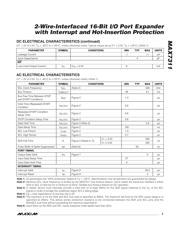
DC ELECTRICAL CHARACTERISTICS (continued)
(V
+
= 2V to 5.5V, T
A
= -40°C to +125°C, unless otherwise noted. Typical values are at V
+
= 3.3V, T
A
= +25°C.) (Note 1)
PARAMETER SYM B O L CONDITIONS MIN TYP MAX UNITS
Leakage Current -1 +1 µA
Input Capacitance 4pF
INT
Low-Level Output Current I
OL
V
OL
= 0.4V 6 mA
AC ELECTRICAL CHARACTERISTICS
(V
+
= 2V to 5.5V, T
A
= -40°C to +125°C, unless otherwise noted.) (Note 1)
PARAMETER SYM B O L CONDITIONS MIN TYP MAX UNITS
SCL Clock Frequency f
SCL
(Note 2) 400 kHz
Bus Timeout t
TIMEOUT
29 61 ms
Bus Free Time Between STOP
and START Conditions
t
BUF
Figure 2 1.3 µs
Hold Time (Repeated) START
Condition
t
HD
,
STA
Figure 2 0.6 µs
Repeated START Condition
Setup Time
t
SU,STA
Figure 2 0.6 µs
STOP Condition Setup Time t
SU
,
STO
Figure 2 0.6 µs
Data Hold Time t
HD
,
DAT
Figure 2 (Note 3) 0.9 µs
Data Setup Time t
SU
,
DAT
Figure 2 100 ns
SCL Low Period t
LOW
Figure 2 1.3 µs
SCL High Period t
HIGH
Figure 2 0.7 µs
V+ < 3.3V 500
SDA Fall Time t
F
Figure 2 (Notes 4, 5)
V+ ≥ 3.3V 250
ns
Pulse Width of Spike Suppressed t
SP
(Note 6) 50 ns
PORT TIMING
Output Data Valid t
PV
Figure 7 3 µs
Input Data Setup Time 27 µs
Input Data Hold Time 0µs
INTERRUPT TIMING
Interrupt Valid t
IV
Figure 9 30.5 µs
Interrupt Reset t
IR
Figure 9 2 µs
器件 Datasheet 文档搜索
AiEMA 数据库涵盖高达 72,405,303 个元件的数据手册,每天更新 5,000 多个 PDF 文件
