Datasheet 搜索 > 逻辑芯片 > ON Semiconductor(安森美) > MC14049UBDTR2G 数据手册 > MC14049UBDTR2G 数据手册 1/100 页

 器件3D模型
¥ 1.532
MC14049UBDTR2G 数据手册 - ON Semiconductor(安森美)
制造商:
ON Semiconductor(安森美)
分类:
逻辑芯片
封装:
TSSOP-16
描述:
六位缓冲器
Pictures:
3D模型
符号图
焊盘图
引脚图
产品图
页面导航:
导航目录
MC14049UBDTR2G数据手册
Page:
of 100 Go
若手册格式错乱,请下载阅览PDF原文件

Document Number: MC33910
Rev. 9.0, 7/2016
NXP Semiconductors
Technical Data
© 2016 NXP B.V.
LIN system basis chip with
high-side drivers
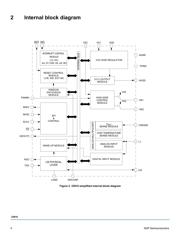
The 33910G5/BAC is a SMARTMOS Serial Peripheral Interface (SPI) controlled
System Basis Chip (SBC), combining many frequently used functions in an MCU
based system, plus a Local Interconnect Network (LIN) transceiver. The 33910
has a 5.0 V, 50 mA/60 mA low dropout regulator with full protection and reporting
features. The device provides full SPI readable diagnostics and a selectable
timing watchdog for detecting errant operation. The LIN Protocol Specification
2.0 and 2.1 compliant LIN transceiver has waveshaping circuitry which can be
disabled for higher data rates.
Two 50 mA/60 mA high-side switches with optional pulse-width modulated
(PWM) are implemented to drive small loads. One high voltage input is available
for use in contact monitoring, or as external wake-up input. This input can be
used as high voltage Analog Input. The voltage on this pin is divided by a
selectable ratio and available via an analog multiplexer.
The 33910 has three main operating modes: Normal (all functions available),
Sleep (V
DD
off, wake-up via LIN, wake-up inputs (L1), cyclic sense and forced
wake-up), and Stop (V
DD
on with limited current capability, wake-up via CS, LIN
bus, wake-up inputs, cyclic sense, forced wake-up and external reset).
The 33910 is compatible with LIN Protocol Specification 2.0, 2.1, and
SAEJ2602-2.
Features
• Full-duplex SPI interface at frequencies up to 4.0 MHz
• LIN transceiver capable of up to 100 kbps with wave shaping
•Two 50 mA/60 mA high-side switches
• One high voltage analog/logic Input
• Configurable window watchdog
•5.0 V low drop regulator with fault detection and low voltage reset (LVR)
circuitry
• Switched/protected 5.0 V output (used for Hall sensors)
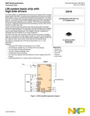
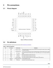
Figure 1. 33910 simplified application diagram
33910
Applications
• Window lift
• Mirror switch
•Door lock
• Sunroof
• Light control
AC SUFFIX (Pb-FREE)
98ASH70029A
32-PIN LQFP
SYSTEM BASIS CHIP WITH LIN
2
ND
GENERATION
33910
MCU
LIN INTERFACE
VS1
VS2
VSENSE
HS1
L1
HVDD
HS2
WDCONF
AGND
LGND
PGND
LIN
VDD
PWMIN
ADOUT0
MOSI
MISO
SCLK
CS
RXD
TXD
IRQ
RST
V
BAT
MC33910G5AC/MC3433910G5AC
器件 Datasheet 文档搜索
AiEMA 数据库涵盖高达 72,405,303 个元件的数据手册,每天更新 5,000 多个 PDF 文件
