Datasheet 搜索 > 触发器 > ON Semiconductor(安森美) > MC14076BDR2 数据手册 > MC14076BDR2 数据手册 1/7 页
 器件3D模型
¥ 0
MC14076BDR2 数据手册 - ON Semiconductor(安森美)
制造商:
ON Semiconductor(安森美)
分类:
触发器
封装:
SOIC-16
描述:
4位D类寄存器具有三态输出 4-Bit D-Type Register with Three-State Outputs
Pictures:
3D模型
符号图
焊盘图
引脚图
产品图
页面导航:
导航目录
MC14076BDR2数据手册
Page:
of 7 Go
若手册格式错乱,请下载阅览PDF原文件
© Semiconductor Components Industries, LLC, 2014
August, 2014 − Rev. 8
1 Publication Order Number:
MC14076B/D
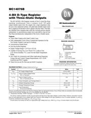
MC14076B
4-Bit D-Type Register
with Three-State Outputs
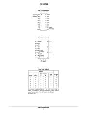
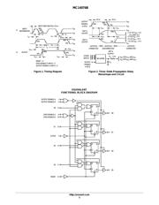
The MC14076B 4−Bit Register consists of four D−type flip−flops
operating synchronously from a common clock. OR gated
output−disable inputs force the outputs into a high−impedance state
for use in bus organized systems. OR gated data−disable inputs cause
the Q outputs to be fed back to the D inputs of the flip−flops. Thus they
are inhibited from changing state while the clocking process remains
undisturbed. An asynchronous master root is provided to clear all four
flip−flops simultaneously independent of the clock or disable inputs.
Features
• Three−State Outputs with Gated Control Lines
• Fully Independent Clock Allows Unrestricted Operation for the
Two Modes: Parallel Load and Do Nothing
• Asynchronous Master Reset
• Four Bus Buffer Registers
• Supply Voltage Range = 3.0 Vdc to 18 Vdc
• Capable of Driving Two Low−Power TTL Loads or One
Low−Power Schottky TTL Load Over the Rated Temperature
Range
• NLV Prefix for Automotive and Other Applications Requiring
Unique Site and Control Change Requirements; AEC−Q100
Qualified and PPAP Capable
• These Devices are Pb−Free and are RoHS Compliant
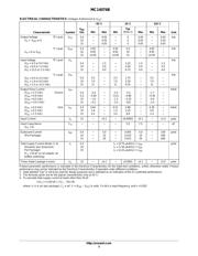
MAXIMUM RATINGS (Voltages Referenced to V
SS
)
Symbol
Parameter Value Unit
V
DD
DC Supply Voltage Range −0.5 to +18.0 V
V
in
, V
out
Input or Output Voltage Range
(DC or Transient)
−0.5 to V
DD
+ 0.5 V
I
in
, I
out
Input or Output Current
(DC or Transient) per Pin
±10 mA
P
D
Power Dissipation, per Package (Note 1) 500 mW
T
A
Ambient Temperature Range −55 to +125 °C
T
stg
Storage Temperature Range −65 to +150 °C
T
L
Lead Temperature
(8−Second Soldering)
260 °C
Stresses exceeding those listed in the Maximum Ratings table may damage the device. If any of these limits are exceeded, device functionality
should not be assumed, damage may occur and reliability may be affected.
1. Temperature Derating: “D/DW” Packages: –7.0 mW/_C From 65_C To 125_C
This device contains protection circuitry to guard against damage due to high static voltages or electric fields. However, precautions must be
taken to avoid applications of any voltage higher than maximum rated voltages to this high−impedance circuit. For proper operation, V
in
and V
out
should be constrained to the range V
SS
≤ (V
in
or V
out
) ≤ V
DD
.
Unused inputs must always be tied to an appropriate logic voltage level (e.g., either V
SS
or V
DD
). Unused outputs must be left open.
http://onsemi.com
MARKING DIAGRAM
SOIC−16
D SUFFIX
CASE 751B
14076BG
AWLYWW
A = Assembly Location
WL, L = Wafer Lot
YY, Y = Year
WW, W = Work Week
G = Pb−Free Package
See detailed ordering and shipping information in the package
dimensions section on page 6 of this data sheet.
ORDERING INFORMATION
1
16
器件 Datasheet 文档搜索
AiEMA 数据库涵盖高达 72,405,303 个元件的数据手册,每天更新 5,000 多个 PDF 文件
