Datasheet 搜索 > 稳压芯片 > Microchip(微芯) > MCP1825S-1202E/DB 数据手册 > MCP1825S-1202E/DB 数据手册 16/38 页

¥ 4.69
MCP1825S-1202E/DB 数据手册 - Microchip(微芯)
制造商:
Microchip(微芯)
分类:
稳压芯片
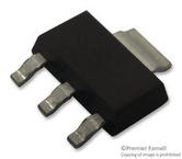
封装:
TO-261-4
描述:
MICROCHIP MCP1825S-1202E/DB 固定电压稳压器, LDO, 2.1V至6V, 210mV压差, 1.2V输出, 500mA输出, SOT-223-3
Pictures:
3D模型
符号图
焊盘图
引脚图
产品图
页面导航:
引脚图在P16Hot
典型应用电路图在P3P19P20P21
原理图在P4P5P6
标记信息在P23P24
封装信息在P23P25P26P28P29P32P35
技术参数、封装参数在P8P9P10
应用领域在P1P3
电气规格在P8P9P18P19
导航目录
MCP1825S-1202E/DB数据手册
Page:
of 38 Go
若手册格式错乱,请下载阅览PDF原文件
MCP1825/MCP1825S
DS22056B-page 16 © 2008 Microchip Technology Inc.
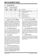
3.0 PIN DESCRIPTION
The descriptions of the pins are listed in Table 3-1.
TABLE 3-1: PIN FUNCTION TABLE
3.1 Shutdown Control Input (SHDN)
The SHDN input is used to turn the LDO output voltage
on and off. When the SHDN input is at a logic-high
level, the LDO output voltage is enabled. When the
SHDN
input is pulled to a logic-low level, the LDO
output voltage is disabled. When the SHDN input is
pulled low, the PWRGD output also goes low and the
LDO enters a low quiescent current shutdown state
where the typical quiescent current is 0.1 µA.
3.2 Input Voltage Supply (V
IN
)
Connect the unregulated or regulated input voltage
source to V
IN
. If the input voltage source is located
several inches away from the LDO, or the input source
is a battery, it is recommended that an input capacitor
be used. A typical input capacitance value of 1 µF to
10 µF should be sufficient for most applications.
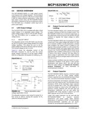
3.3 Ground (GND)
Connect the GND pin of the LDO to a quiet circuit
ground. This will help the LDO power supply rejection
ratio and noise performance. The ground pin of the
LDO only conducts the quiescent current of the LDO
(typically 120 µA), so a heavy trace is not required.
For applications that have switching or noisy inputs, tie
the GND pin to the return of the output capacitor.
Ground planes help lower inductance and voltage
spikes caused by fast transient load currents and are
recommended for applications that are subjected to
fast load transients.
3.4 Regulated Output Voltage (V
OUT
)
The V
OUT
pin is the regulated output voltage of the
LDO. A minimum output capacitance of 1.0 µF is
required for LDO stability. The MCP1825/MCP1825S
is stable with ceramic, tantalum and aluminum-electro-
lytic capacitors. See Section 4.3 “Output Capacitor”
for output capacitor selection guidance.
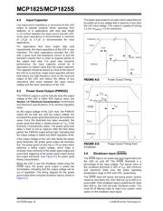
3.5 Power Good Output (PWRGD)
The PWRGD output is an open-drain output used to
indicate when the LDO output voltage is within 92%
(typically) of its nominal regulation value. The PWRGD
threshold has a typical hysteresis value of 2%. The
PWRGD output is delayed by 110 µs (typical) from the
time the LDO output is within 92% + 3% (maximum
hysteresis) of the regulated output value on power-up.
This delay time is internally fixed.
3.6 Output Voltage Adjust Input (ADJ)
For adjustable applications, the output voltage is
connected to the ADJ input through a resistor divider
that sets the output voltage regulation value. This
provides the user the capability to set the output
voltage to any value they desire within the 0.8V to 5.0V
range of the device.
3.7 Exposed Pad (EP)
The DDPAK and TO-220 package have an exposed
tab on the package. A heat sink may may be mount to
the tab to aid in the removal of heat from the package
during operation. The exposed tab is at the ground
potential of the LDO.
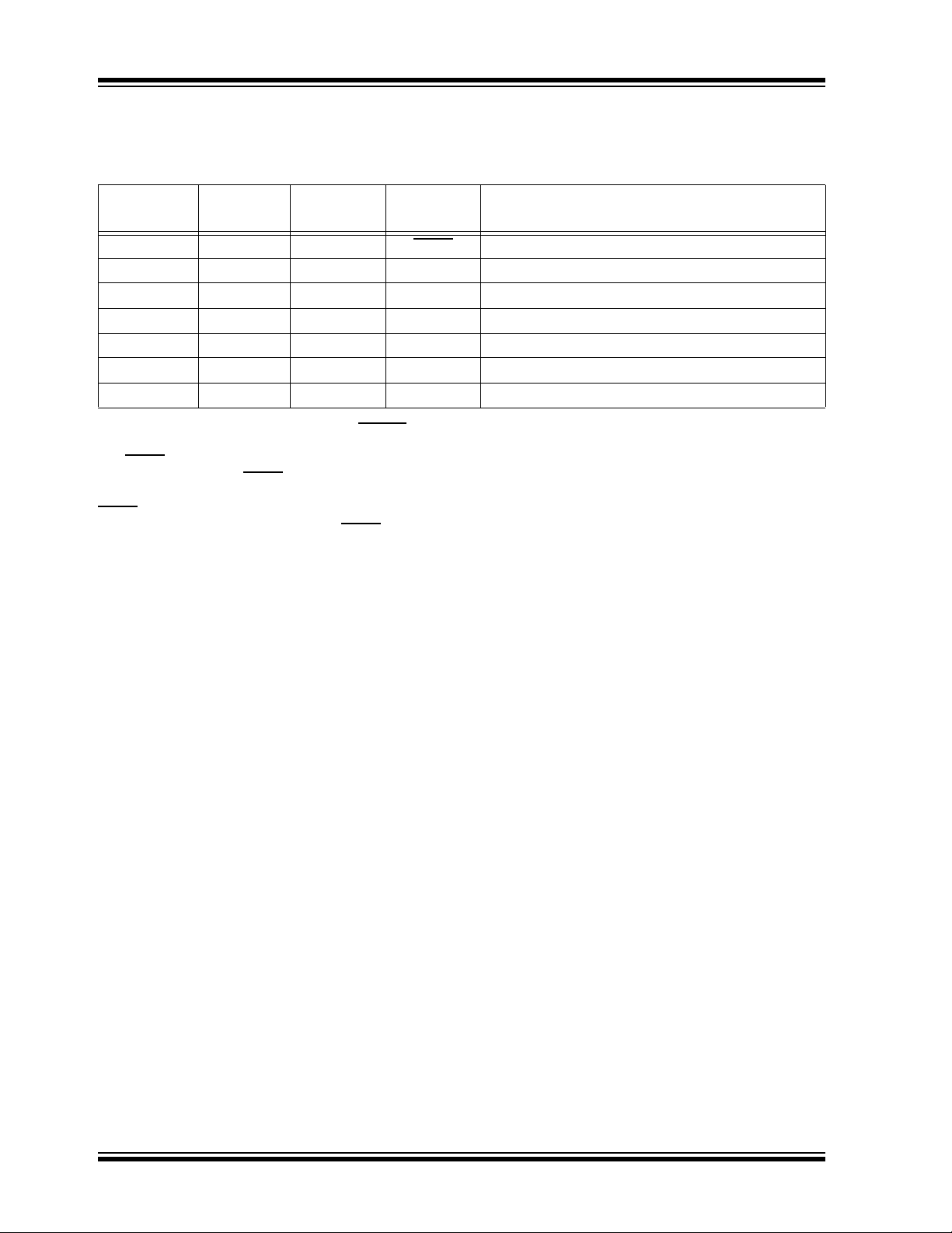
3-Pin Fixed
Output
5-Pin Fixed
Output
Adjustable
Output
Name Description
—
11SHDNShutdown Control Input (active-low)
122V
IN
Input Voltage Supply
2 3 3 GND Ground
344V
OUT
Regulated Output Voltage
—
5
—
PWRGD Power Good Output
——
5 ADJ Voltage Adjust/Sense Input
Exposed Pad Exposed Pad Exposed Pad EP Exposed Pad of the Package (ground potential)
器件 Datasheet 文档搜索
AiEMA 数据库涵盖高达 72,405,303 个元件的数据手册,每天更新 5,000 多个 PDF 文件
