Datasheet 搜索 > 稳压芯片 > Microchip(微芯) > MCP1825S-1202E/DB 数据手册 > MCP1825S-1202E/DB 数据手册 18/38 页

¥ 4.692
MCP1825S-1202E/DB 数据手册 - Microchip(微芯)
制造商:
Microchip(微芯)
分类:
稳压芯片
封装:
TO-261-4
描述:
MICROCHIP MCP1825S-1202E/DB 固定电压稳压器, LDO, 2.1V至6V, 210mV压差, 1.2V输出, 500mA输出, SOT-223-3
Pictures:
3D模型
符号图
焊盘图
引脚图
产品图
页面导航:
引脚图在P16Hot
典型应用电路图在P3P19P20P21
原理图在P4P5P6
标记信息在P23P24
封装信息在P23P25P26P28P29P32P35
技术参数、封装参数在P8P9P10
应用领域在P1P3
电气规格在P8P9P18P19
导航目录
MCP1825S-1202E/DB数据手册
Page:
of 38 Go
若手册格式错乱,请下载阅览PDF原文件
MCP1825/MCP1825S
DS22056B-page 18 © 2008 Microchip Technology Inc.
4.4 Input Capacitor
Low input source impedance is necessary for the LDO
output to operate properly. When operating from
batteries, or in applications with long lead length
(> 10 inches) between the input source and the LDO,
some input capacitance is recommended. A minimum
of 1.0 µF to 4.7 µF is recommended for most
applications.
For applications that have output step load
requirements, the input capacitance of the LDO is very
important. The input capacitance provides the LDO
with a good local low-impedance source to pull the
transient currents from in order to respond quickly to
the output load step. For good step response
performance, the input capacitor should be of
equivalent (or higher) value than the output capacitor.
The capacitor should be placed as close to the input of
the LDO as is practical. Larger input capacitors will also
help reduce any high-frequency noise on the input and
output of the LDO and reduce the effects of any
inductance that exists between the input source
voltage and the input capacitance of the LDO.
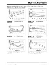
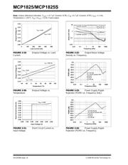
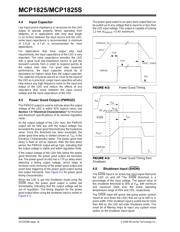
4.5 Power Good Output (PWRGD)
The PWRGD output is used to indicate when the output
voltage of the LDO is within 92% (typical value, see
Section 1.0 “Electrical Characteristics” for Minimum
and Maximum specifications) of its nominal regulation
value.
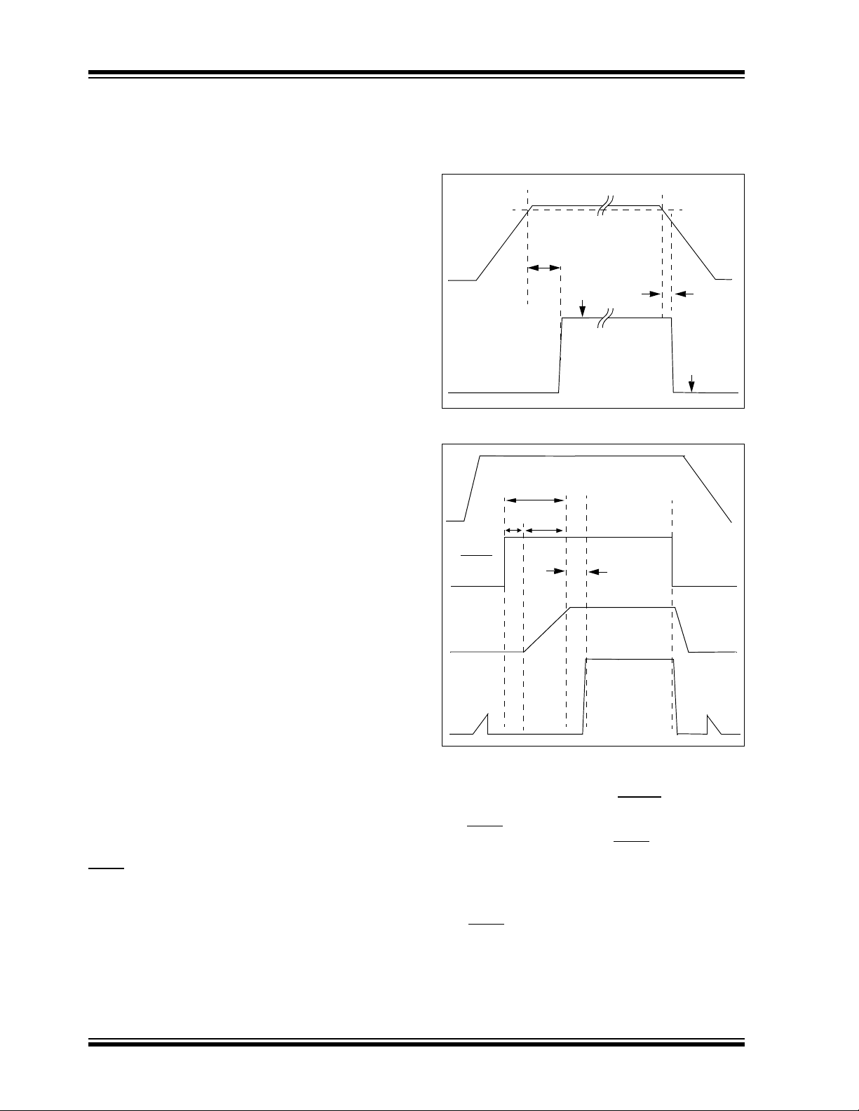
As the output voltage of the LDO rises, the PWRGD
output will be held low until the output voltage has
exceeded the power good threshold plus the hysteresis
value. Once this threshold has been exceeded, the
power good time delay is started (shown as T
PG
in the
Electrical Characteristics table). The power good time
delay is fixed at 110 µs (typical). After the time delay
period, the PWRGD output will go high, indicating that
the output voltage is stable and within regulation limits.
If the output voltage of the LDO falls below the power
good threshold, the power good output will transition
low. The power good circuitry has a 170 µs delay when
detecting a falling output voltage, which helps to
increase noise immunity of the power good output and
avoid false triggering of the power good output during
fast output transients. See Figure 4-2 for power good
timing characteristics.
When the LDO is put into Shutdown mode using the
SHDN
input, the power good output is pulled low
immediately, indicating that the output voltage will be
out of regulation. The timing diagram for the power
good output when using the shutdown input is shown in
Figure 4-3.
The power good output is an open-drain output that can
be pulled up to any voltage that is equal to or less than
the LDO input voltage. This output is capable of sinking
1.2 mA (V
PWRGD
< 0.4V maximum).
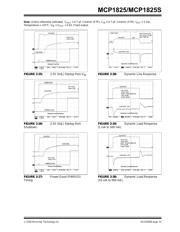
FIGURE 4-2: Power Good Timing.
FIGURE 4-3: Power Good Timing from
Shutdown.
4.6 Shutdown Input (SHDN)
The SHDN input is an active-low input signal that turns
the LDO on and off. The SHDN
threshold is a
percentage of the input voltage. The typical value of
this shutdown threshold is 30% of V
IN
, with minimum
and maximum limits over the entire operating
temperature range of 45% and 15%, respectively.
The SHDN
input will ignore low-going pulses (pulses
meant to shut down the LDO) that are up to 400 ns in
pulse width. If the shutdown input is pulled low for more
than 400 ns, the LDO will enter Shutdown mode. This
small bit of filtering helps to reject any system noise
spikes on the shutdown input signal.
TPG
TVDET_PWRG
VPWRGD_TH
VOUT
PWRGD
VOL
VOH
V
IN
SHDN
V
OUT
30 µs
70 µs
T
OR
PWRGD
T
PG
器件 Datasheet 文档搜索
AiEMA 数据库涵盖高达 72,405,303 个元件的数据手册,每天更新 5,000 多个 PDF 文件
