Datasheet 搜索 > Microchip(微芯) > MCP3901A0T-E/ML 数据手册 > MCP3901A0T-E/ML 数据手册 4/62 页
 器件3D模型
¥ 5.099
MCP3901A0T-E/ML 数据手册 - Microchip(微芯)
制造商:
Microchip(微芯)
封装:
QFN-20
Pictures:
3D模型
符号图
焊盘图
引脚图
产品图
页面导航:
导航目录
MCP3901A0T-E/ML数据手册
Page:
of 62 Go
若手册格式错乱,请下载阅览PDF原文件
MCP3901
DS22192D-page 4 © 2011 Microchip Technology Inc.
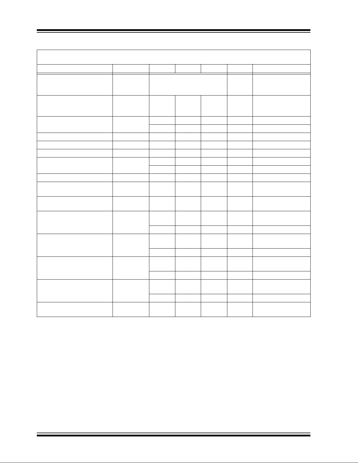
Output Data Rate f
D
See Tab le 4- 2 ksps f
D
= DRCLK = DMCLK/
OSR = MCLK/
(4 x PRESCALE x OSR)
Analog Input Absolute Voltage
on CH0+, CH0-, CH1+,
CH1- Pins
CHn+ -1 — +1 V All analog input
channels, measured to
AGND (Note 7)
Analog Input Leakage Current A
IN
—1—nA(Note 4)
—2—nA-40°C < T
A
< 125°C
Differential Input Voltage Range (CHn+ – CHn-) — — 500/GAIN mV (Note 1)
Offset Error (Note 2) V
OS
-3 — +3 mV (Note 6)
Offset Error Drift — 3 — µV/°C From -40°C to +125°C
Gain Error (Note 2) GE — -0.4 — % G = 1
-2.5 — +2.5 % All Gains
Gain Error Drift — 1 — ppm/°C From -40°C to +125°C
Integral Nonlinearity (Note 2) INL — 15 — ppm GAIN = 1,
DITHER = On
Input Impedance Z
IN
350 — — kΩ Proportional to
1/AMCLK
Signal-to-Noise and Distortion
Ratio (Notes 2, 3)
SINAD 89 91 — dB OSR = 256,
DITHER = On
78 79 — dB
Total Harmonic Distortion
(Notes 2, 3)
THD — -104 -102 dB OSR = 256,
DITHER = On
—-85-84dB
Signal-to-Noise Ratio
(Notes 2, 3)
SNR 89 91 — dB OSR = 256,
DITHER = On
80 81 — dB
Spurious Free Dynamic Range
(Note 2)
SFDR — 109 — dB OSR = 256,
DITHER = On
—87—dB
Crosstalk (50/60 Hz) (Note 2) CTALK — -133 — dB OSR = 256,
DITHER = On
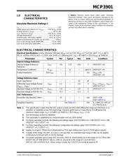
ELECTRICAL CHARACTERISTICS (CONTINUED)
Electrical Specifications: Unless otherwise indicated, AV
DD
= 4.5 to 5.5V, DV
DD
= 2.7 to 5.5V; -40°C < T
A
< +85°C,
MCLK = 4 MHz; PRESCALE = 1; OSR = 64; GAIN = 1; Dithering OFF; V
IN
= -0.5 dBFS = 333 mV
RMS
@ 50/60 Hz
Parameters Symbol Min Typical Max Units Conditions
Note 1: This specification implies that the ADC output is valid over this entire differential range and that there is no
distortion or instability across this input range. Dynamic performance is specified at -0.5 dB below the
maximum signal range, V
IN
= -0.5 dBFS @ 50/60 Hz = 353 mV
RMS,
V
REF
= 2.4V.
2: See terminology section for definition.
3: This parameter is established by characterization and not 100% tested.
4: For these operating currents, the following bit settings apply: SHUTDOWN<1:0> = 00, RESET<1:0> = 00,
VREFEXT = 0, CLKEXT = 0.
5: For these operating currents, the following Configuration bit settings apply: SHUTDOWN<1:0> = 11,
VREFEXT = 1, CLKEXT = 1.
6: Applies to all gains. Offset error is dependant on PGA gain setting (see Figure 2-19 for typical values).
7: Outside of this range, the ADC accuracy is not specified. An extended input range of ±6V can be applied
continuously to the part with no risk for damage.
8: For proper operation and to keep ADC accuracy, AMCLK should always be in the range of 1 to 5 MHz with
BOOST bits off. With BOOST bits on, AMCLK should be in the range of 1 to 8.192 MHz,
AMCLK = MCLK/PRESCALE. When using a crystal, the CLKEXT bit should be equal to ‘0’.
器件 Datasheet 文档搜索
AiEMA 数据库涵盖高达 72,405,303 个元件的数据手册,每天更新 5,000 多个 PDF 文件
