Datasheet 搜索 > ON Semiconductor(安森美) > ML6428CS1X 数据手册 > ML6428CS1X 数据手册 4/10 页
 器件3D模型
¥ 3.124
ML6428CS1X 数据手册 - ON Semiconductor(安森美)
制造商:
ON Semiconductor(安森美)
封装:
SOIC-8
Pictures:
3D模型
符号图
焊盘图
引脚图
产品图
页面导航:
导航目录
ML6428CS1X数据手册
Page:
of 10 Go
若手册格式错乱,请下载阅览PDF原文件

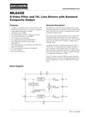
ML6428 DATA SHEET
4
REV. 1C April 2004
Functional Description
The ML6428 is a dual monolithic continuous time video
filter designed for reconstructing the luminance and
chrominance signals from an S-Video D/A source.
Composite video output is generated by summing the Y
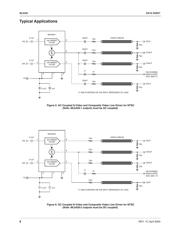
and C outputs. The ML6428CS-1 is intended for use in AC
coupled input and output applications. The ML6428CS-2 is
intended for AC coupled input and DC coupled output
applications (see Figures 5 and 6).
The filters have a 4th-order Butterworth characteristic with
an optimization toward low overshoot and flat group delay.
All outputs are capable of driving 2VP-P into 150
Ω
video
loads, with up to 35pF of load capacitance at the output pin.
ML6428CS-1 outputs are AC coupled, ML6428CS-2 outputs
are DC coupled. The CV output can drive two video loads
plus a high-impedance modulator. Thus the CV output is
intended to simultaneously drive a VCR, a TV, and a high-
impedance modulator. Y and C are capable of driving a 75
Ω
load at 1VP-P. The ML6428 is capable of driving two com-
posite loads and a TV modulator simultaneously.
All channels are clamped during sync to establish the appro-
priate output voltage swing range. Thus the input coupling
capacitors do not behave according to the conventional RC
time constant. Clamping for all channels settles within 2ms
of a change in video input sources.
In most applications, the ML6428's input coupling capacitors
are 0.1µF. The Y input sinks 1.6µA during active video,
which nominally tilts a horizontal line by 2mV (max) at
the Y output (Figure 4). During sync, the clamp typically
sources 20µA to restore the DC level. The net result is that
the average input current is zero.
Any change in the input coupling capacitor's value will
inversely alter the amount of tilt per line. Such a change
will also linearly affect the clamp response times.
The C channel has no pulldown current sources and is essen-
tially tilt-free. Its input is clamped by a feedback amp which
responds to the CV output. Since CV = Y+C, the CV output
will droop by the same amount as Y during active video, and
will rise by the same amount as Y during sync.
The ML6428 is robust and stable under all stated load and
input conditions. Capacitavely bypassing both VCC pins
directly to ground ensures this performance. (See Figures 5
and 6)
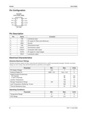
Luminance (Y) I/O
The luma input is driven by either a low impedance source of
1VP-P or the output of a 75
Ω
terminated line. The input is
required to be AC coupled via a 0.1uF coupling capacitor
which allows for a nominal settling time of 2ms. The luma
output is capable of driving a 150
Ω
load at 2VP-P or 1VP-P
into a 75
Ω
load. ML6428CS-1 outputs are AC coupled,
ML6428CS-2 outputs are DC coupled.Up to 35pF of load
capacitance (at the output pin) can be driven without stability
or slew issues. A 220µF AC coupling capacitor is recom-
mended at the output (ML6428-1 only).
Chrominance (C) I/O
The chroma input is driven by a low impedance source of
0.7VP-P or the output of a 75
Ω
terminated line. The input is
required to be AC coupled via a 0.1uF coupling capacitor
which allows for a nominal clamping time of 1ms. The
chroma output is capable of driving a 150
Ω
load at 2VP-P
or 1VP-P into a 75
Ω
load. ML6428CS-1 outputs are AC
coupled, ML6428CS-2 outputs are DC coupled. Up to 35pF
of load capacitance can be driven without stability or slew
issues. A 220µF AC coupling capacitor is recommended at
the output (ML6428-1 only).
Composite video (CV) output
The composite video output is capable of driving 2 CV loads
to 2VP-P and a high input impedance CV modulator.
ML6428CS-1 outputs are AC coupled, ML6428CS-2 outputs
are DC coupled. It is intended to drive three devices: TV,
VCR, and a modulator. The TV or VCR input can be shorted
to ground and the other outputs will still meet specifications.
Up to 35pF of load capacitance (at the output pin) can be
driven without stability or slew issues.
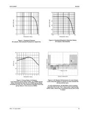
Using the ML6428 for PAL Applications
The ML6428 can be optimized for PAL video by adding
frequency peaking to the composite and S-video outputs.
Figures 7 and 8 illustrate the use of a additional external
capacitor, 330pF, added in parallel to the output source
termination resistor. This raises the frequency response from
1.6 dB down at 4.8Mhz to 0.35dB down at 4.8MHz allowing
for accurate reproduction of the upper sideband of the PAL
subcarrier. Figure 9 shows the frequency response of PAL
video with various values of peaking capacitors (0pF, 220pF,
270pF, 330pF) between 0 and 10MHz.
For NTSC applications without the peaking capacitor the
rejection at 27MHz is 42dB (typical) while for PAL applica-
tions with the peaking capacitor the rejection at 27MHz is
38dB (typical). This is shown in Figure 10. The differential
group delay is shown in Figure 11 with and without a peak-
ing capacitor (0pF, 220pF, 270pF, and 330pF) varies slightly
with capacitance, going from 8ns to 13ns.
器件 Datasheet 文档搜索
AiEMA 数据库涵盖高达 72,405,303 个元件的数据手册,每天更新 5,000 多个 PDF 文件
