Datasheet 搜索 > RAM芯片 > Micron(镁光) > MT41J128M16JT-093G:K TR 数据手册 > MT41J128M16JT-093G:K TR 数据手册 1/215 页


¥ 49.122
MT41J128M16JT-093G:K TR 数据手册 - Micron(镁光)
制造商:
Micron(镁光)
分类:
RAM芯片
封装:
TFBGA-96
Pictures:
3D模型
符号图
焊盘图
引脚图
产品图
页面导航:
原理图在P14P15P150
封装尺寸在P22P23P24P25
标记信息在P1P2
功能描述在P12P13P150P196
技术参数、封装参数在P26P27P31P32P33P34P35P36P37P38P39P40
电气规格在P26P27P31P32P33P34P35P36P37P38P39P40
型号编号列表在P2
导航目录
MT41J128M16JT-093G:K TR数据手册
Page:
of 215 Go
若手册格式错乱,请下载阅览PDF原文件
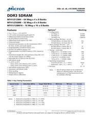
DDR3 SDRAM
MT41J512M4 – 64 Meg x 4 x 8 Banks
MT41J256M8 – 32 Meg x 8 x 8 Banks
MT41J128M16 – 16 Meg x 16 x 8 Banks
Features
•V
DD
= V
DDQ
= 1.5V ±0.075V
• 1.5V center-terminated push/pull I/O
• Differential bidirectional data strobe
•8n-bit prefetch architecture
• Differential clock inputs (CK, CK#)
• 8 internal banks
• Nominal and dynamic on-die termination (ODT)
for data, strobe, and mask signals
• Programmable CAS READ latency (CL)
• Posted CAS additive latency (AL)
• Programmable CAS WRITE latency (CWL) based on
t
CK
• Fixed burst length (BL) of 8 and burst chop (BC) of 4
(via the mode register set [MRS])
• Selectable BC4 or BL8 on-the-fly (OTF)
• Self refresh mode
•T
C
of 0°C to 95°C
– 64ms, 8192 cycle refresh at 0°C to 85°C
– 32ms, 8192 cycle refresh at 85°C to 95°C
• Self refresh temperature (SRT)
• Automatic self refresh (ASR)
• Write leveling
• Multipurpose register
• Output driver calibration
Options
1
Marking
• Configuration
– 512 Meg x 4 512M4
– 256 Meg x 8 256M8
– 128 Meg x 16 128M16
• FBGA package (Pb-free) – x4, x8
– 78-ball (8mm x 10.5mm) Rev. K DA
– 78-ball (8mm x 10.5mm) Rev. N EF
• FBGA package (Pb-free) – x16
– 96-ball (8mm x 14mm) Rev. K JT
– 96-ball (8mm x 14mm) Rev. N TW
• Timing – cycle time
– 938ps @ CL = 14 (DDR3-2133) -093
– 1.07ns @ CL = 13 (DDR3-1866) -107
– 1.25ns @ CL = 11 (DDR3-1600) -125
– 1.5ns @ CL = 9 (DDR3-1333) -15E
– 1.87ns @ CL = 7 (DDR3-1066) -187E
• Operating temperature
– Commercial (0°C ≤ T
C
≤ +95°C) None
– Industrial (–40°C ≤ T
C
≤ +95°C) IT
• Revision :K / :N
Note:
1. Not all options listed can be combined to
define an offered product. Use the part
catalog search on http://www.micron.com
for available offerings.
Table 1: Key Timing Parameters
Speed Grade Data Rate (MT/s) Target
t
RCD-
t
RP-CL
t
RCD (ns)
t
RP (ns) CL (ns)
-093
1, 2, 3, 4
2133 14-14-14 13.13 13.13 13.13
-107
1, 2, 3
1866 13-13-13 13.91 13.91 13.91
-125
1, 2,
1600 11-11-11 13.75 13.75 13.75
-15E
1,
1333 9-9-9 13.5 13.5 13.5
-187E 1066 7-7-7 13.1 13.1 13.1
Notes:
1. Backward compatible to 1066, CL = 7 (-187E).
2. Backward compatible to 1333, CL = 9 (-15E).
3. Backward compatible to 1600, CL = 11 (-125).
4. Backward compatible to 1866, CL = 13 (-107).
2Gb: x4, x8, x16 DDR3 SDRAM
Features
PDF: 09005aef826aaadc
2Gb_DDR3_SDRAM.pdf - Rev. S 02/16 EN
1
Micron Technology, Inc. reserves the right to change products or specifications without notice.
© 2006 Micron Technology, Inc. All rights reserved.
Products and specifications discussed herein are subject to change by Micron without notice.
器件 Datasheet 文档搜索
AiEMA 数据库涵盖高达 72,405,303 个元件的数据手册,每天更新 5,000 多个 PDF 文件
