Datasheet 搜索 > RAM芯片 > Micron(镁光) > MT41J128M16JT-093G:K TR 数据手册 > MT41J128M16JT-093G:K TR 数据手册 4/215 页


¥ 49.122
MT41J128M16JT-093G:K TR 数据手册 - Micron(镁光)
制造商:
Micron(镁光)
分类:
RAM芯片
封装:
TFBGA-96
Pictures:
3D模型
符号图
焊盘图
引脚图
产品图
页面导航:
原理图在P14P15P150
封装尺寸在P22P23P24P25
标记信息在P1P2
功能描述在P12P13P150P196
技术参数、封装参数在P26P27P31P32P33P34P35P36P37P38P39P40
电气规格在P26P27P31P32P33P34P35P36P37P38P39P40
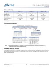
型号编号列表在P2
导航目录
MT41J128M16JT-093G:K TR数据手册
Page:
of 215 Go
若手册格式错乱,请下载阅览PDF原文件

Input Clock Frequency Change ...................................................................................................................... 127
Write Leveling ............................................................................................................................................... 129
Write Leveling Procedure ........................................................................................................................... 131
Write Leveling Mode Exit Procedure ........................................................................................................... 133
Initialization ................................................................................................................................................. 134
Mode Registers .............................................................................................................................................. 136
Mode Register 0 (MR0) ................................................................................................................................... 137
Burst Length ............................................................................................................................................. 137
Burst Type ................................................................................................................................................. 138
DLL RESET ................................................................................................................................................ 139
Write Recovery .......................................................................................................................................... 140
Precharge Power-Down (Precharge PD) ...................................................................................................... 140
CAS Latency (CL) ....................................................................................................................................... 140
Mode Register 1 (MR1) ................................................................................................................................... 142
DLL ENABLE/DISABLE .............................................................................................................................. 142
Output Drive Strength ............................................................................................................................... 143
OUTPUT ENABLE/DISABLE ...................................................................................................................... 143
TDQS ENABLE .......................................................................................................................................... 143
On-Die Termination (ODT) ........................................................................................................................ 144
WRITE LEVELING ..................................................................................................................................... 144
Posted CAS Additive Latency (AL) ............................................................................................................... 144
Mode Register 2 (MR2) ................................................................................................................................... 146
CAS WRITE Latency (CWL) ........................................................................................................................ 146
AUTO SELF REFRESH (ASR) ....................................................................................................................... 147
SELF REFRESH TEMPERATURE (SRT) ........................................................................................................ 147
SRT versus ASR .......................................................................................................................................... 148
Dynamic On-Die Termination (ODT) ......................................................................................................... 148
Mode Register 3 (MR3) ................................................................................................................................... 149
MULTIPURPOSE REGISTER (MPR) ............................................................................................................ 149
MPR Functional Description ...................................................................................................................... 150
MPR Address Definitions and Bursting Order .............................................................................................. 151
MPR Read Predefined Pattern .................................................................................................................... 156
MODE REGISTER SET (MRS) Command ........................................................................................................ 156
ZQ CALIBRATION Operation ......................................................................................................................... 157
ACTIVATE Operation ..................................................................................................................................... 158
READ Operation ............................................................................................................................................ 160
WRITE Operation .......................................................................................................................................... 171
DQ Input Timing ....................................................................................................................................... 179
PRECHARGE Operation ................................................................................................................................. 181
SELF REFRESH Operation .............................................................................................................................. 181
E
xtended Temperature Usage ........................................................................................................................ 183
Power-Down Mode ........................................................................................................................................ 184
RESET Operation ........................................................................................................................................... 192
On-Die Termination (ODT) ............................................................................................................................ 194
Functional Representation of ODT ............................................................................................................. 194
Nominal ODT ............................................................................................................................................ 194
Dynamic ODT ............................................................................................................................................... 196
Dynamic ODT Special Use Case ................................................................................................................. 196
Functional Description .............................................................................................................................. 196
Synchronous ODT Mode ................................................................................................................................ 202
ODT Latency and Posted ODT .................................................................................................................... 202
Timing Parameters .................................................................................................................................... 202
2Gb: x4, x8, x16 DDR3 SDRAM
Features
PDF: 09005aef826aaadc
2Gb_DDR3_SDRAM.pdf - Rev. S 02/16 EN
4
Micron Technology, Inc. reserves the right to change products or specifications without notice.
© 2006 Micron Technology, Inc. All rights reserved.
器件 Datasheet 文档搜索
AiEMA 数据库涵盖高达 72,405,303 个元件的数据手册,每天更新 5,000 多个 PDF 文件
