Datasheet 搜索 > Motorola(摩托罗拉) > MTD5P06V-T4 数据手册 > MTD5P06V-T4 数据手册 1/7 页


¥ 0
MTD5P06V-T4 数据手册 - Motorola(摩托罗拉)
制造商:
Motorola(摩托罗拉)
Pictures:
3D模型
符号图
焊盘图
引脚图
产品图
页面导航:
导航目录
MTD5P06V-T4数据手册
Page:
of 7 Go
若手册格式错乱,请下载阅览PDF原文件
© Semiconductor Components Industries, LLC, 2006
July, 2006 − Rev. 6
1 Publication Order Number:
MTD5P06V/D
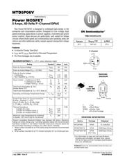
MTD5P06V
Preferred Device
Power MOSFET
5 Amps, 60 Volts P−Channel DPAK
This Power MOSFET is designed to withstand high energy in the
avalanche and commutation modes. Designed for low voltage, high
speed switching applications in power supplies, converters and power
motor controls, these devices are particularly well suited for bridge
circuits where diode speed and commutating safe operating areas are
critical and offer additional safety margin against unexpected voltage
transients.
Features
• Avalanche Energy Specified
• I
DSS
and V
DS(on)
Specified at Elevated Temperature
• Pb−Free Packages are Available
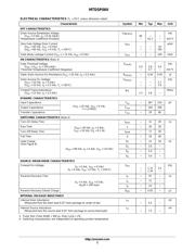
MAXIMUM RATINGS (T
C
= 25°C unless otherwise noted)
Rating Symbol Value Unit
Drain−to−Source Voltage V
DSS
60 Vdc
Drain−to−Gate Voltage (R
GS
= 1.0 MW)
V
DGR
60 Vdc
Gate−to−Source Voltage
− Continuous
− Non−repetitive (t
p
≤ 10 ms)
V
GS
V
GSM
± 15
± 25
Vdc
Vpk
Drain Current − Continuous @ 25°C
− Continuous @ 100°C
− Single Pulse (t
p
≤ 10 ms)
I
D
I
D
I
DM
5
4
18
Adc
Apk
Total Power Dissipation @ 25°C
Derate above 25°C
Total Power Dissipation @ T
A
= 25°C (Note 2
)
P
D
40
0.27
2.1
W
W/°C
W
Operating and Storage Temperature Range T
J
, T
stg
−55 to
175
°C
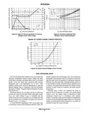
Single Pulse Drain−to−Source Avalanche
Energy − Starting T
J
= 25°C
(V
DD
= 25 Vdc, V
GS
= 10 Vdc, Peak
I
L
= 5 Apk, L = 10 mH, R
G
= 25 W)
E
AS
125 mJ
Thermal Resistance
Junction−to−Case
Junction−to−Ambient (Note 1)
Junction−to−Ambient (Note 2)
R
q
JC
R
q
JA
R
q
JA
3.75
100
71.4
°C/W
Maximum Lead Temperature for Soldering
Purposes, 1/8″ from Case for 10 seconds
T
L
260 °C
Stresses exceeding Maximum Ratings may damage the device. Maximum
Ratings are stress ratings only. Functional operation above the Recommended
Operating Conditions is not implied. Extended exposure to stresses above the
Recommended Operating Conditions may affect device reliability.
1. When surface mounted to an FR4 board using the minimum recommended
pad size.
2. When surface mounted to an FR−4 board using the 0.5 sq in drain pad size.
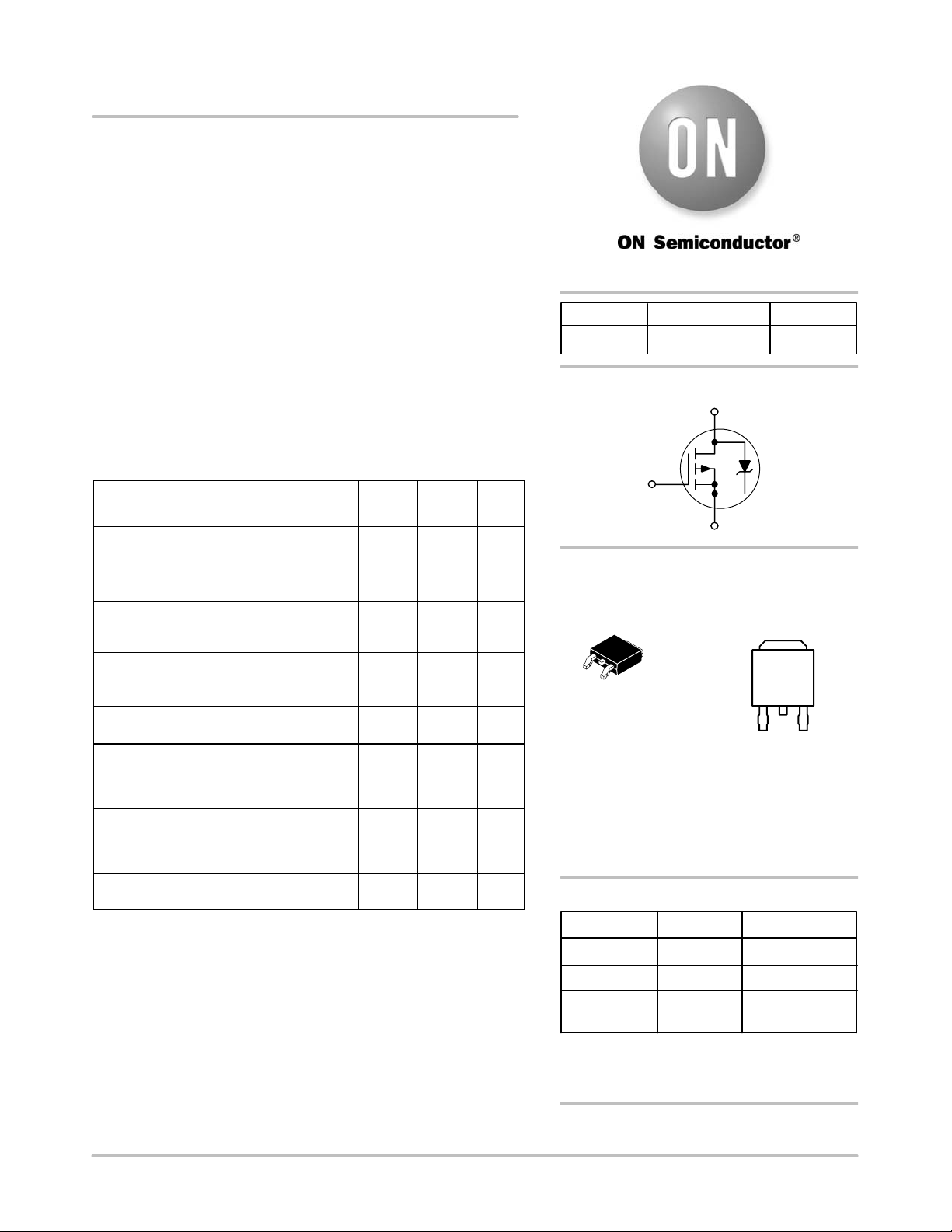
D
S
G
P−Channel
Preferred devices are recommended choices for future use
and best overall value.
http://onsemi.com
60 V
340 mW
R
DS(on)
TYP
5.0 A
I
D
MAXV
(BR)DSS
1
Gate
3
Source
2
Drain
4
Drain
DPAK
CASE 369C
STYLE 2
MARKING
DIAGRAM
Y = Year
WW = Work Week
5P06V = Device Code
G = Pb−Free Package
1
2
3
4
Device Package Shipping
†
ORDERING INFORMATION
MTD5P06V DPAK 75 Units/Rail
MTD5P06VT4 DPAK 2500/Tape & Ree
l
YWW
5
P06VG
MTD5P06VT4G DPAK
(Pb−Free)
2500/Tape & Ree
l
†For information on tape and reel specifications,
including part orientation and tape sizes, please
refer to our Tape and Reel Packaging Specification
s
Brochure, BRD8011/D.
器件 Datasheet 文档搜索
AiEMA 数据库涵盖高达 72,405,303 个元件的数据手册,每天更新 5,000 多个 PDF 文件
