Datasheet 搜索 > Motorola(摩托罗拉) > MTD5P06E 数据手册 > MTD5P06E 数据手册 1/10 页


¥ 0
MTD5P06E 数据手册 - Motorola(摩托罗拉)
制造商:
Motorola(摩托罗拉)
封装:
CASE 369A-13
Pictures:
3D模型
符号图
焊盘图
引脚图
产品图
MTD5P06E数据手册
Page:
of 10 Go
若手册格式错乱,请下载阅览PDF原文件
www.DataSheet4U.com
1
Motorola TMOS Power MOSFET Transistor Device Data
P–Channel Enhancement–Mode Silicon Gate
This advanced TMOS E–FET is designed to withstand high
energy in the avalanche and commutation modes. The new energy
efficient design also offers a drain–to–source diode with a fast
recovery time. Designed for low voltage, high speed switching
applications in power supplies, converters and PWM motor
controls, these devices are particularly well suited for bridge circuits
where diode speed and commutating safe operating areas are
critical and offer additional safety margin against unexpected
voltage transients.
• Avalanche Energy Specified
• Source–to–Drain Diode Recovery Time Comparable to a Discrete
Fast Recovery Diode
• Diode is Characterized for Use in Bridge Circuits
• I
DSS
and V
DS(on)
Specified at Elevated Temperature
• Surface Mount Package Available in 16 mm, 13–inch/2500
Unit Tape & Reel, Add T4 Suffix to Part Number
• Replaces MTD4P05 and MTD4P06E
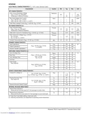
MAXIMUM RATINGS
(T
C
= 25°C unless otherwise noted)
Rating
Symbol Value Unit
Drain–Source Voltage V
DSS
60 Vdc
Drain–Gate Voltage (R
GS
= 1.0 MΩ) V
DGR
60 Vdc
Gate–Source Voltage — Continuous
Gate–Source Voltage — Non–Repetitive (t
p
≤ 10 ms)
V
GS
V
GSM
± 20
± 30
Vdc
Vpk
Drain Current — Continuous
— Continuous @ 100°C
— Single Pulse (t
p
≤ 10 µs)
I
D
I
D
I
DM
5.0
3.8
15
Adc
Apk
Total Power Dissipation
Derate above 25°C
Total Power Dissipation @ T
A
= 25°C, when mounted to minimum recommended pad size
P
D
40
0.32
1.75
Watts
W/°C
Watts
Operating and Storage Temperature Range T
J
, T
stg
–55 to 150 °C
Single Pulse Drain–to–Source Avalanche Energy — Starting T
J
= 25°C
(V
DD
= 25 Vdc, V
GS
= 10 Vdc, I
L
= 5.0 Apk, L = 10 mH, R
G
= 25 Ω)
E
AS
125
mJ
Thermal Resistance — Junction to Case
— Junction to Ambient
— Junction to Ambient, when mounted to minimum recommended pad size
R
θJC
R
θJA
R
θJA
3.13
100
71.4
°C/W
Maximum Temperature for Soldering Purposes, 1/8″ from case for 10 seconds T
L
260 °C
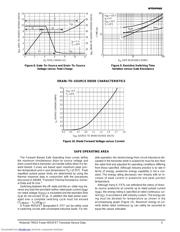
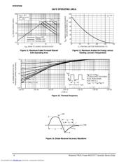
Designer’s Data for “Worst Case” Conditions — The Designer’s Data Sheet permits the design of most circuits entirely from the information presented. SOA Limit
curves — representing boundaries on device characteristics — are given to facilitate “worst case” design.
E–FET and Designer’s are trademarks of Motorola, Inc. TMOS is a registered trademark of Motorola, Inc.
Thermal Clad is a trademark of the Bergquist Company.
Preferred devices are Motorola recommended choices for future use and best overall value.
REV 1
Order this document
by MTD5P06E/D
SEMICONDUCTOR TECHNICAL DATA
Motorola, Inc. 1995
TMOS POWER FET
5.0 AMPERES
60 VOLTS
R
DS(on)
= 0.55 OHM
Motorola Preferred Device
D
S
G
CASE 369A–13, Style 2
DPAK
Downloaded from Elcodis.com electronic components distributor
器件 Datasheet 文档搜索
AiEMA 数据库涵盖高达 72,405,303 个元件的数据手册,每天更新 5,000 多个 PDF 文件
