Datasheet 搜索 > 开发套件 > ON Semiconductor(安森美) > NCP2809BGEVB 数据手册 > NCP2809BGEVB 数据手册 4/24 页

¥ 817.189
NCP2809BGEVB 数据手册 - ON Semiconductor(安森美)
制造商:
ON Semiconductor(安森美)
分类:
开发套件
封装:
-
描述:
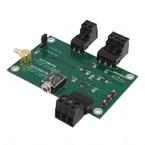
ON SEMICONDUCTOR NCP2809BGEVB 评估板, NCP2809 135mW 立体声耳机放大器
Pictures:
3D模型
符号图
焊盘图
引脚图
产品图
页面导航:
引脚图在P1Hot
典型应用电路图在P1P2P3P17
原理图在P2P3P17P18P20
封装尺寸在P23P24
焊盘布局在P23P24
型号编码规则在P1P22P24
标记信息在P1P22
封装信息在P22
功能描述在P4
技术参数、封装参数在P22
应用领域在P1
电气规格在P5P6

导航目录
NCP2809BGEVB数据手册
Page:
of 24 Go
若手册格式错乱,请下载阅览PDF原文件
NCP2809 Series
http://onsemi.com
4
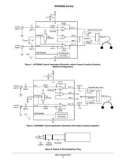
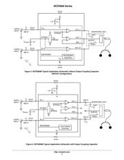
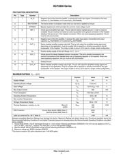
PIN FUNCTION DESCRIPTION
Pin Type Symbol Description
1 I IN_R Negative input of the second amplifier. It receives the audio input signal. Connected to the input
capicator C
in
(NCP2809A) or the external R
in
(NCP2809B).
2 I SHUTDOWN The device enters in shutdown mode when a a low level is applied on this pin.
3 I BYPASS Bypass capacitor pin which provides the common mode voltage (V
P
/2).
4 O REF_I Virtual ground amplifier feed back. This pin sets the stereo headset ground. In order to improve
crosstalk, this pin must be connected as close as possible to the ground connection of the headset
(ideally at the ground pin of the headset connector). When one uses bypassing capacitors, this pin
must be left unconnected.
5 I IN_L Negative input of the first amplifier. It receives the audio input signal. Connected to the input
capacitor C
in
(NCP2809A) or the external R
in
(NCP2809B).
6 O OUT_L Stereo headset amplifier analog output left. This pin will output the amplified analog signal and,
depending on the application, must be coupled with a capacitor or directly connected to the left
loudspeaker of the headset. This output is able to drive a 16 load in a single−ended configuration.
7 I V
P
Positive analog supply of the cell. Range: 2.2 V – 5.5 V
8 O OUT_I Virtual ground for stereo Headset common connection. This pin is directly connected to the
common connection of the headset when use of bypassing capacitor is not required. When one
uses bypassing capacitors, this pin must be left unconnected.
9 I V
M
Analog Ground
10 O OUT_R Stereo headset amplifier analog output right. This pin will output the amplified analog signal and,
depending on the application, must be coupled with a capacitor or directly connected to the right
loudspeaker of the headset. This output is able to drive a 16 load in a single−ended configuration.
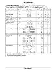
MAXIMUM RATINGS (T
A
= +25°C)
Rating Symbol Value Unit
Supply Voltage V
p
6.0 V
Operating Supply Voltage O
p
V
p
2.2 to 5.5 V
Input Voltage V
in
−0.3 to V
CC
+ 0.3 V
Max Output Current I
out
250 mA
Power Dissipation P
d
Internally Limited −
Operating Ambient Temperature T
A
−40 to +85 °C
Max Junction Temperature T
J
150 °C
Storage Temperature Range T
stg
−65 to +150 °C
Thermal Resistance, Junction−to−Air Micro10
UDFN
R
JA
200
240
°C/W
ESD Protection Human Body Model (HBM) (Note 1)
Machine Model (MM) (Note 2)
− 8000
200
V
Latch up current at Ta = 85_C (Note 3) ±100 mA
Stresses exceeding Maximum Ratings may damage the device. Maximum Ratings are stress ratings only. Functional operation above the
Recommended Operating Conditions is not implied. Extended exposure to stresses above the Recommended Operating Conditions may affect
device reliability.
1. Human Body Model, 100 pF discharged through a 1.5 k resistor following specification JESD22/A114 8.0 kV can be applied on OUT_L,
OUT_R, REF_I and OUT_I outputs. For other pins, 2.0 kV is the specified voltage.
2. Machine Model, 200 pF discharged through all pins following specification JESD22/A115.
3. Maximum ratings per JEDEC standard JESD78.
*This device contains 752 active transistors and 1740 MOS gates.
器件 Datasheet 文档搜索
AiEMA 数据库涵盖高达 72,405,303 个元件的数据手册,每天更新 5,000 多个 PDF 文件
