Datasheet 搜索 > DC/DC转换器 > ON Semiconductor(安森美) > NCP3170ADR2G 数据手册 > NCP3170ADR2G 数据手册 2/28 页
 器件3D模型
¥ 1.801
NCP3170ADR2G 数据手册 - ON Semiconductor(安森美)
制造商:
ON Semiconductor(安森美)
分类:
DC/DC转换器
封装:
SOIC-8
描述:
ON SEMICONDUCTOR NCP3170ADR2G 直流-直流开关降压(逐步递减)稳压器, 可调, 4.5V-18V输入, 1.25V-5V输出, 3A输出, SOIC-8
Pictures:
3D模型
符号图
焊盘图
引脚图
产品图
页面导航:
引脚图在P1Hot
典型应用电路图在P1
原理图在P2
封装尺寸在P26
焊盘布局在P26
型号编码规则在P1P28
标记信息在P1P26P28
封装信息在P1
功能描述在P2
技术参数、封装参数在P1P3
应用领域在P1
电气规格在P4P5P6P7
型号编号列表在P3
导航目录
NCP3170ADR2G数据手册
Page:
of 28 Go
若手册格式错乱,请下载阅览PDF原文件
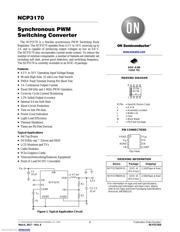
NCP3170
www.onsemi.com
2
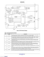
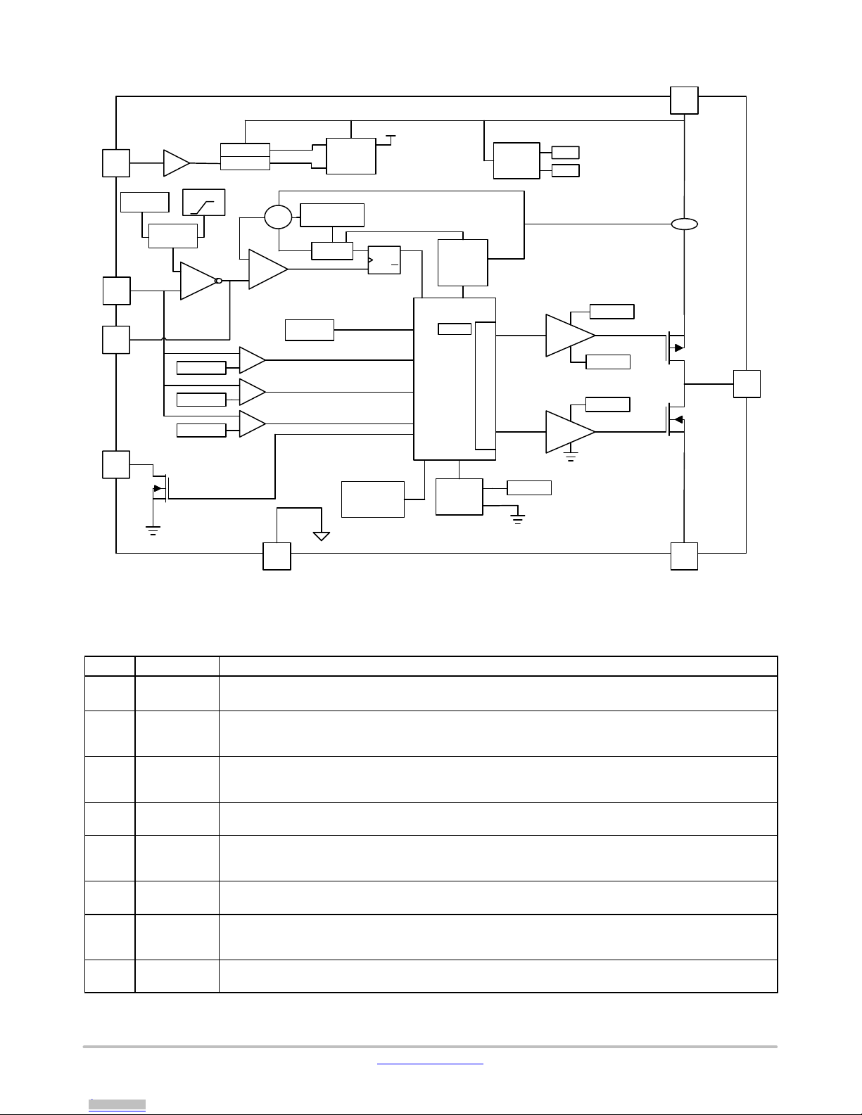
Figure 2. NCP3170 Block Diagram
hs
EN
UVLO
POR
Power
Control
(PC)
VDD
Driver
Voltage
Clamp
VCV
VCL
VIN
0.030 V/A
Current
Sense
Reference
ORing
Circuit
Soft Start
FB
COMP
PG
+
−
+
−
S
Slope
Compensation
Oscillator
S
SET
Q
R
CLR
Q
Soft Start
Complete
998 mV
867 mV
728 mV
+
−
+
−
+
−
AGND
Over
Temperature
Protection
Zero
Current
Detection
VSW
PGND
NDRV
PDRV
VIN
VCW
VCL
Logic
HS
LS
Pulse by
Pulse
Current
Limit
VSW
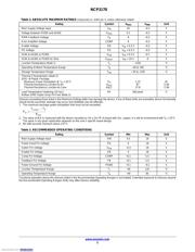
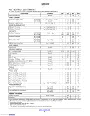
Table 1. PIN FUNCTION DESCRIPTION
Pin Pin Name Description
1 PGND The power ground pin is the high current path for the device. The pin should be soldered to a large copper
area to reduce thermal resistance. PGND needs to be electrically connected to AGND.
2 VIN The input voltage pin powers the internal control circuitry and is monitored by multiple voltage comparators.
The VIN pin is also connected to the internal power PMOS switch and linear regulator output. The VIN pin
has high di/dt edges and must be decoupled to ground close to the pin of the device.
3 AGND
The analog ground pin serves as small-signal ground. All small-signal ground paths should connect to the
AGND pin and should also be electrically connected to power ground at a single point, avoiding any high
current ground returns.
4 FB Inverting input to the OTA error amplifier. The FB pin in conjunction with the external compensation serves to
stabilize and achieve the desired output voltage with current mode compensation.
5 COMP The loop compensation pin is used to compensate the transconductance amplifier which stabilizes the
operation of the converter stage. Place compensation components as close to the converter as possible.
Connect a RC network between COMP and AGND to compensate the control loop.
6 EN Enable pin. Pull EN to logic high to enable the device. Pull EN to logic low to disable the device. Do not leave
it open.
7 PG
Power good is an open drain 500 mA pull down indicating output voltage is within the power good window. If
the power good function is not used, it can be connected to the VSW node to reduce thermal resistance. Do
not connect PG to the VSW node if the application is turning on into pre-bias.
8 VSW The VSW pin is the connection of the drains of the internal N and P MOSFETS. At switch off, the inductor will
drive this pin below ground as the body diode and the NMOS conducts with a high dv/dt.
Downloaded from Arrow.com.Downloaded from Arrow.com.
器件 Datasheet 文档搜索
AiEMA 数据库涵盖高达 72,405,303 个元件的数据手册,每天更新 5,000 多个 PDF 文件
