Datasheet 搜索 > DC/DC转换器 > ON Semiconductor(安森美) > NCP3170ADR2G 数据手册 > NCP3170ADR2G 数据手册 4/28 页
 器件3D模型
¥ 1.801
NCP3170ADR2G 数据手册 - ON Semiconductor(安森美)
制造商:
ON Semiconductor(安森美)
分类:
DC/DC转换器
封装:
SOIC-8
描述:
ON SEMICONDUCTOR NCP3170ADR2G 直流-直流开关降压(逐步递减)稳压器, 可调, 4.5V-18V输入, 1.25V-5V输出, 3A输出, SOIC-8
Pictures:
3D模型
符号图
焊盘图
引脚图
产品图
页面导航:
引脚图在P1Hot
典型应用电路图在P1
原理图在P2
封装尺寸在P26
焊盘布局在P26
型号编码规则在P1P28
标记信息在P1P26P28
封装信息在P1
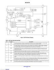
功能描述在P2
技术参数、封装参数在P1P3
应用领域在P1
电气规格在P4P5P6P7
型号编号列表在P3
导航目录
NCP3170ADR2G数据手册
Page:
of 28 Go
若手册格式错乱,请下载阅览PDF原文件
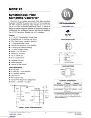
NCP3170
www.onsemi.com
4
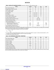
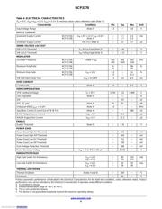
Table 4. ELECTRICAL CHARACTERISTICS
(T
A
= 25°C, V
IN
= V
EN
= 12 V, V
OUT
= 3.3 V for min/max values unless otherwise noted (Note 7))
Characteristic
Conditions Min Typ Max Unit
Input Voltage Range (Note 5) 4.5 − 18 V
SUPPLY CURRENT
Quiescent Supply Current NCP3170A
NCP3170B
V
IN
= EN = 12 V V
FB
= 0.8 V
(Note 5)
−
−
1.7
1.7
2.0
2.0
mA
Shutdown Supply Current EN = 0 V (Note 5) − 13 17
mA
UNDER VOLTAGE LOCKOUT
VIN UVLO Threshold
V
IN
Rising Edge (Note 5) − 4.41 − V
VIN UVLO Threshold V
IN
Falling Edge (Note 5) − 4.13 − V
MODULATOR
Oscillator Frequency NCP3170A
NCP3170B
Enable = V
IN
450
900
500
1000
550
1100
kHz
Maximum Duty Ratio NCP3170A
NCP3170B
91
90
−
−
96
96
%
Minimum Duty Ratio NCP3170A
NCP3170B
V
IN
= 12 V 6.0
4.0
−
−
11
11.5
%
VIN Soft Start Ramp Time V
FB
= VCOMP 3.5 4.6 6.0 ms
OVER CURRENT
Current Limit (Note 4) 4.0 − 6.0 A
PWM COMPENSATION
VFB Feedback Voltage T
A
= 25°C 0.792 0.8 0.808 V
Line Regulation (Note 4) − 1 − %
GM − 201 −
mS
AOL DC gain (Note 4) 40 55 − dB
Unity Gain BW (C
OUT
= 10 pF) (Note 4) 2.0 − − MHz
Input Bias Current (Current Out of FB IB Pin) (Note 4) − − 286 nA
IEAOP Output Source Current V
FB
= 0 V − 20.1 −
mA
IEAOM Output Sink Current V
FB
= 2 V − 21.3 −
mA
ENABLE
Enable Threshold (Note 5) − 1.41 − V
POWER GOOD
Power Good High On Threshold − 875 − mV
Power Good High Off Threshold − 859 − mV
Power Good Low On Threshold − 712 − mV
Power Good Low Off Threshold − 728 − mV
Over Voltage Protection Threshold − 998 − mV
Power Good Low Voltage
V
IN
= 12 V, IPG = 500 mA
− 0.195 − V
PWM OUTPUT STAGE
High-Side Switch On-Resistance
V
IN
= 12 V
V
IN
= 4.5 V
−
−
90
100
130
150
mW
Low-Side Switch On-Resistance V
IN
= 12 V
V
IN
= 4.5 V
−
−
25
29
35
39
mW
THERMAL SHUTDOWN
Thermal Shutdown (Notes 4 and 6) − 164 − °C
Hysteresis − 43 − °C
Product parametric performance is indicated in the Electrical Characteristics for the listed test conditions, unless otherwise noted. Product
performance may not be indicated by the Electrical Characteristics if operated under different conditions.
4. Guaranteed by design
5. Ambient temperature range of −40°C to +85°C.
6. This is not a protection feature.
7. The device is not guaranteed to operate beyond the maximum operating ratings.
Downloaded from Arrow.com.Downloaded from Arrow.com.Downloaded from Arrow.com.Downloaded from Arrow.com.
器件 Datasheet 文档搜索
AiEMA 数据库涵盖高达 72,405,303 个元件的数据手册,每天更新 5,000 多个 PDF 文件
