Datasheet 搜索 > 稳压芯片 > ON Semiconductor(安森美) > NCP500SN30T1G 数据手册 > NCP500SN30T1G 数据手册 14/20 页

¥ 0.919
NCP500SN30T1G 数据手册 - ON Semiconductor(安森美)
制造商:
ON Semiconductor(安森美)
分类:
稳压芯片
封装:
TSOT-23-5
描述:
LDO) 线性电压调节器,150mA,3.0V 至 3.5V,ON Semiconductor### LDO(低压降)线性电压调节器,ON Semiconductor低压降或 LDO 为线性电压稳压器。 我们有多种系列的线性稳压器。 LDO 稳压器可在输入 - 输出差分电压较小时运行。 LDO 电压稳压器可提供快速瞬态响应、宽输入电压范围、低静态电流、低噪声、高 PSRR。
Pictures:
3D模型
符号图
焊盘图
引脚图
产品图
页面导航:
引脚图在P2Hot
典型应用电路图在P2P14
原理图在P2
封装尺寸在P18P19
焊盘布局在P18P19
型号编码规则在P2P17P20
标记信息在P1P2P17P18P19P20
封装信息在P17
功能描述在P3
技术参数、封装参数在P17
应用领域在P2P13P17
电气规格在P3P4P5P6P7
型号编号列表在P3
导航目录
NCP500SN30T1G数据手册
Page:
of 20 Go
若手册格式错乱,请下载阅览PDF原文件
NCP500, NCV500
www.onsemi.com
13
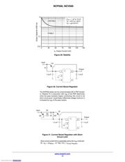
The maximum dissipation the package can handle is
given by:
PD +
T
J(max)
*T
A
R
qJA
If T
J
is not recommended to exceed 125°C, then the
NCP500 can dissipate up to 400 mW @ 25°C.
The power dissipated by the NCP500 can be calculated
from the following equation:
P
tot
+
ƪ
V
in
*I
gnd
(I
out
)
ƫ
)
[
V
in
* V
out
]
*I
out
or
V
inMAX
+
P
tot
)
V
out
*
I
out
I
gnd
) I
out
If a 150 mA output current is needed the ground current
is extracted from the data sheet curves: 200 mA @ 150 mA.
For a NCP500SN18T1 (1.8 V), the maximum input voltage
will then be 4.4 V, good for a 1 Cell Li−ion battery.
Hints
Please be sure the V
in
and GND lines are sufficiently wide.
When the impedance of these lines is high, there is a chance
to pick up noise or cause the regulator to malfunction.
Set external components, especially the output capacitor,
as close as possible to the circuit, and make leads as short
as possible.
Package Placement
DFN packages can be placed using standard pick and
place equipment with an accuracy of "0.05 mm.
Component pick and place systems are composed of a vision
system that recognizes and positions the component and a
mechanical system which physically performs the pick and
place operation. Two commonly used types of vision
systems are: (1) a vision system that locates a package
silhouette and (2) a vision system that locates individual
bumps on the interconnect pattern. The latter type renders
more accurate place but tends to be more expensive and time
consuming. Both methods are acceptable since the parts
align due to a self−centering feature of the DFN solder joint
during solder re−flow.
Solder Paste
Type 3 or Type 4 solder paste is acceptable.
Re−flow and Cleaning
The DFN may be assembled using standard IR/IR
convection SMT re−flow processes without any special
considerations. As with other packages, the thermal profile
for specific board locations must be determined. Nitrogen
purge is recommended during solder for no−clean fluxes.
The DFN is qualified for up to three re−flow cycles at 235°C
peak (J−STD−020). The actual temperature of the DFN is a
function of:
• Component density
• Component location on the board
• Size of surrounding components
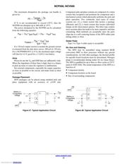
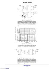
Figure 27. Typical Application Circuit
V
out
Battery or
Unregulated
Voltage
C1
C2
OFF
ON
1
2
3
5
4
+
+
Figure 28. Typical Application Circuit
V
out
Battery or
Unregulated
Voltage
+
C1
OFF
ON
1
3
2
4
5
6
+
C2
Downloaded from Arrow.com.Downloaded from Arrow.com.Downloaded from Arrow.com.Downloaded from Arrow.com.Downloaded from Arrow.com.Downloaded from Arrow.com.Downloaded from Arrow.com.Downloaded from Arrow.com.Downloaded from Arrow.com.Downloaded from Arrow.com.Downloaded from Arrow.com.Downloaded from Arrow.com.Downloaded from Arrow.com.Downloaded from Arrow.com.
器件 Datasheet 文档搜索
AiEMA 数据库涵盖高达 72,405,303 个元件的数据手册,每天更新 5,000 多个 PDF 文件
