Datasheet 搜索 > 稳压芯片 > ON Semiconductor(安森美) > NCP500SN30T1G 数据手册 > NCP500SN30T1G 数据手册 18/20 页

¥ 0.919
NCP500SN30T1G 数据手册 - ON Semiconductor(安森美)
制造商:
ON Semiconductor(安森美)
分类:
稳压芯片
封装:
TSOT-23-5
描述:
LDO) 线性电压调节器,150mA,3.0V 至 3.5V,ON Semiconductor### LDO(低压降)线性电压调节器,ON Semiconductor低压降或 LDO 为线性电压稳压器。 我们有多种系列的线性稳压器。 LDO 稳压器可在输入 - 输出差分电压较小时运行。 LDO 电压稳压器可提供快速瞬态响应、宽输入电压范围、低静态电流、低噪声、高 PSRR。
Pictures:
3D模型
符号图
焊盘图
引脚图
产品图
页面导航:
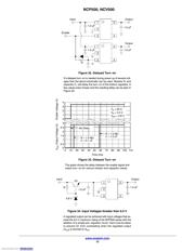
引脚图在P2Hot
典型应用电路图在P2P14
原理图在P2
封装尺寸在P18P19
焊盘布局在P18P19
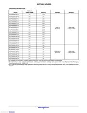
型号编码规则在P2P17P20
标记信息在P1P2P17P18P19P20
封装信息在P17
功能描述在P3
技术参数、封装参数在P17
应用领域在P2P13P17
电气规格在P3P4P5P6P7
型号编号列表在P3
导航目录
NCP500SN30T1G数据手册
Page:
of 20 Go
若手册格式错乱,请下载阅览PDF原文件
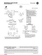
TSOP−5
CASE 483
ISSUE N
DATE 12 AUG 2020
SCALE 2:1
1
5
XXX MG
G
GENERIC
MARKING DIAGRAM*
1
5
0.7
0.028
1.0
0.039
ǒ
mm
inches
Ǔ
SCALE 10:1
0.95
0.037
2.4
0.094
1.9
0.074
*For additional information on our Pb−Free strategy and soldering
details, please download the ON Semiconductor Soldering and
Mounting Techniques Reference Manual, SOLDERRM/D.
SOLDERING FOOTPRINT*
*This information is generic. Please refer to
device data sheet for actual part marking.
Pb−Free indicator, “G” or microdot “ G”,
may or may not be present.
XXX = Specific Device Code
A = Assembly Location
Y = Year
W = Work Week
G = Pb−Free Package
1
5
XXXAYWG
G
Discrete/Logic
Analog
(Note: Microdot may be in either location)
XXX = Specific Device Code
M = Date Code
G = Pb−Free Package
NOTES:
1. DIMENSIONING AND TOLERANCING PER ASME
Y14.5M, 1994.
2. CONTROLLING DIMENSION: MILLIMETERS.
3. MAXIMUM LEAD THICKNESS INCLUDES LEAD FINISH
THICKNESS. MINIMUM LEAD THICKNESS IS THE
MINIMUM THICKNESS OF BASE MATERIAL.
4. DIMENSIONS A AND B DO NOT INCLUDE MOLD
FLASH, PROTRUSIONS, OR GATE BURRS. MOLD
FLASH, PROTRUSIONS, OR GATE BURRS SHALL NOT
EXCEED 0.15 PER SIDE. DIMENSION A.
5. OPTIONAL CONSTRUCTION: AN ADDITIONAL
TRIMMED LEAD IS ALLOWED IN THIS LOCATION.
TRIMMED LEAD NOT TO EXTEND MORE THAN 0.2
FROM BODY.
DIM MIN MAX
MILLIMETERS
A
B
C 0.90 1.10
D 0.25 0.50
G 0.95 BSC
H 0.01 0.10
J 0.10 0.26
K 0.20 0.60
M 0 10
S 2.50 3.00
123
54
S
A
G
B
D
H
C
J
__
0.20
5X
C AB
T0.10
2X
2X
T0.20
NOTE 5
C
SEATING
PLANE
0.05
K
M
DETAIL Z
DETAIL Z
TOP VIEW
SIDE VIEW
A
B
END VIEW
1.35 1.65
2.85 3.15
MECHANICAL CASE OUTLINE
PACKAGE DIMENSIONS
ON Semiconductor and are trademarks of Semiconductor Components Industries, LLC dba ON Semiconductor or its subsidiaries in the United States and/or other countries.
ON Semiconductor reserves the right to make changes without further notice to any products herein. ON Semiconductor makes no warranty, representation or guarantee regarding
the suitability of its products for any particular purpose, nor does ON Semiconductor assume any liability arising out of the application or use of any product or circuit, and specifically
disclaims any and all liability, including without limitation special, consequential or incidental damages. ON Semiconductor does not convey any license under its patent rights nor the
rights of others.
98ARB18753C
DOCUMENT NUMBER:
DESCRIPTION:
Electronic versions are uncontrolled except when accessed directly from the Document Repository.
Printed versions are uncontrolled except when stamped “CONTROLLED COPY” in red.
PAGE 1 OF 1
TSOP−5
© Semiconductor Components Industries, LLC, 2018
www.onsemi.com
Downloaded from Arrow.com.Downloaded from Arrow.com.Downloaded from Arrow.com.Downloaded from Arrow.com.Downloaded from Arrow.com.Downloaded from Arrow.com.Downloaded from Arrow.com.Downloaded from Arrow.com.Downloaded from Arrow.com.Downloaded from Arrow.com.Downloaded from Arrow.com.Downloaded from Arrow.com.Downloaded from Arrow.com.Downloaded from Arrow.com.Downloaded from Arrow.com.Downloaded from Arrow.com.Downloaded from Arrow.com.Downloaded from Arrow.com.
器件 Datasheet 文档搜索
AiEMA 数据库涵盖高达 72,405,303 个元件的数据手册,每天更新 5,000 多个 PDF 文件
