Datasheet 搜索 > 双极性晶体管 > Nexperia(安世) > PBSS4240V,115 数据手册 > PBSS4240V,115 数据手册 3/12 页


¥ 0.806
PBSS4240V,115 数据手册 - Nexperia(安世)
制造商:
Nexperia(安世)
分类:
双极性晶体管
封装:
SOT-666
描述:
NXP PBSS4240V,115 , NPN 晶体管, 2 A, Vce=40 V, HFE:75, 150 MHz, 6引脚 SSMini封装
Pictures:
3D模型
符号图
焊盘图
引脚图
产品图
页面导航:
引脚图在P2Hot
封装尺寸在P7
标记信息在P2
应用领域在P2P8
导航目录
PBSS4240V,115数据手册
Page:
of 12 Go
若手册格式错乱,请下载阅览PDF原文件
2003 Jan 30 3
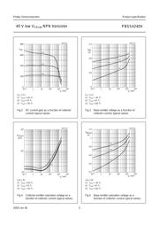
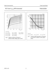
Philips Semiconductors Product specification
40 V low V
CEsat
NPN transistor
PBSS4240V
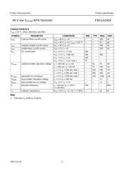
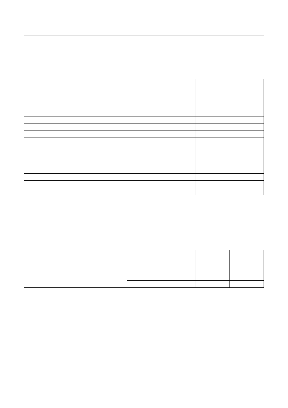
LIMITING VALUES
In accordance with the Absolute Maximum Rating System (IEC 60134).
Notes
1. Device mounted on a ceramic circuit board, Al
2
O
3
, standard footprint.
2. Operated under pulsed conditions: duty cycle δ≤20%, pulse width t
p
≤ 30 ms.
3. Device mounted on a printed-circuit board, single-sided copper, tinplated, standard footprint.
4. Device mounted on a printed-circuit board, single-sided copper, tinplated, mounting pad for collector 1 cm
2
.
THERMAL CHARACTERISTICS
Notes
1. Device mounted on a printed-circuit board, single-sided copper, tinplated, standard footprint.
2. Device mounted on a printed-circuit board, single-sided copper, tinplated, mounting pad for collector 1 cm
2
.
3. Device mounted on a ceramic circuit board, Al
2
O
3
, standard footprint.
4. Operated under pulsed conditions: duty cycle δ≤20%, pulse width t
p
≤ 30 ms.
Soldering
The only recommended soldering method is reflow soldering.
SYMBOL PARAMETER CONDITIONS MIN. MAX. UNIT
V
CBO
collector-base voltage open emitter − 40 V
V
CEO
collector-emitter voltage open base − 40 V
V
EBO
emitter-base voltage open collector − 5V
I
C
collector current (DC) note 1 − 2A
I
CRP
repetitive peak collector current note 2 − 2A
I
CM
peak collector current − 3A
I
B
base current (DC) − 300 mA
I
BM
peak base current − 1A
P
tot
total power dissipation T
amb
≤ 25 °C; note 3 − 300 mW
T
amb
≤ 25 °C; note 4 − 500 mW
T
amb
≤ 25 °C; note 1 − 900 mW
T
amb
≤ 25 °C; notes 2 and 3 − 1.2 W
T
stg
storage temperature −65 +150 °C
T
j
junction temperature − 150 °C
T
amb
operating ambient temperature −65 +150 °C
SYMBOL PARAMETER CONDITIONS VALUE UNIT
R
th j-a
thermal resistance from junction to
ambient
note 1 410 K/W
note 2 215 K/W
note 3 140 K/W
notes 1 and 4 110 K/W
器件 Datasheet 文档搜索
AiEMA 数据库涵盖高达 72,405,303 个元件的数据手册,每天更新 5,000 多个 PDF 文件
