Datasheet 搜索 > Microchip(微芯) > PIC16F1827T-E/SS 数据手册 > PIC16F1827T-E/SS 数据手册 140/406 页
 器件3D模型
¥ 0
PIC16F1827T-E/SS 数据手册 - Microchip(微芯)
制造商:
Microchip(微芯)
封装:
SSOP-20
描述:
18 /20/ 28引脚闪存单片机采用纳瓦XLP技术 18/20/28-Pin Flash Microcontrollers with nanoWatt XLP Technology
Pictures:
3D模型
符号图
焊盘图
引脚图
产品图
页面导航:
引脚图在P6P11P12P13P14P131P204P206P213P322Hot
典型应用电路图在P137P323
原理图在P10P16P52P63P73P97P131P135P139P154P158P164
封装尺寸在P384
标记信息在P383
封装信息在P383P385P386P390P391
功能描述在P315
技术参数、封装参数在P54P58P84P98P102P135P140P146P150P153P167P168
应用领域在P47P54P55P215P222
电气规格在P54P58P84P98P135P140P146P150P153P167P169P175
导航目录
PIC16F1827T-E/SS数据手册
Page:
of 406 Go
若手册格式错乱,请下载阅览PDF原文件

PIC16(L)F1826/27
DS41391D-page 140 2011 Microchip Technology Inc.
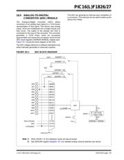
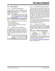
16.1 ADC Configuration
When configuring and using the ADC the following
functions must be considered:
• Port configuration
• Channel selection
• ADC voltage reference selection
• ADC conversion clock source
• Interrupt control
• Result formatting
16.1.1 PORT CONFIGURATION
The ADC can be used to convert both analog and
digital signals. When converting analog signals, the I/O
pin should be configured for analog by setting the
associated TRIS and ANSEL bits. Refer to
Section 12.0 “I/O Ports” for more information.
16.1.2 CHANNEL SELECTION
There are up to 15 channel selections available:
•AN<11:0> pins
• Temperature Indicator
• DAC Output
• FVR (Fixed Voltage Reference) Output
Refer to Section 14.0 “Fixed Voltage Reference
(FVR)”and Section 15.0 “Temperature Indicator
Module” for more information on these channel selec-
tions.
The CHS bits of the ADCON0 register determine which
channel is connected to the sample and hold circuit.
When changing channels, a delay is required before
starting the next conversion. Refer to Section 16.2
“ADC Operation” for more information.
16.1.3 ADC VOLTAGE REFERENCE
The ADPREF bits of the ADCON1 register provides
control of the positive voltage reference. The positive
voltage reference can be:
•V
REF+ pin
•V
DD
• FVR 2.048V
• FVR 4.096V (Not available on LF devices)
The ADNREF bits of the ADCON1 register provides
control of the negative voltage reference. The negative
voltage reference can be:
•V
REF- pin
•V
SS
See Section 14.0 “Fixed Voltage Reference (FVR)”
for more details on the fixed voltage reference.
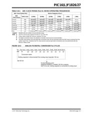
16.1.4 CONVERSION CLOCK
The source of the conversion clock is software select-
able via the ADCS bits of the ADCON1 register. There
are seven possible clock options:
•F
OSC/2
•FOSC/4
•FOSC/8
•F
OSC/16
•FOSC/32
•FOSC/64
•F
RC (dedicated internal oscillator)
The time to complete one bit conversion is defined as
TAD. One full 10-bit conversion requires 11.5 TAD peri-
ods as shown in Figure 16-2.
For correct conversion, the appropriate T
AD specifica-
tion must be met. Refer to the A/D conversion require-
ments in Section 30.0 “Electrical Specifications”for
more information. Table 16-1 gives examples of appro-
priate ADC clock selections.
Note: Analog voltages on any pin that is defined
as a digital input may cause the input buf-
fer to conduct excess current.
Note: Unless using the FRC, any changes in the
system clock frequency will change the
ADC clock frequency, which may
adversely affect the ADC result.
器件 Datasheet 文档搜索
AiEMA 数据库涵盖高达 72,405,303 个元件的数据手册,每天更新 5,000 多个 PDF 文件
