Datasheet 搜索 > Microchip(微芯) > PIC16F1827T-E/SS 数据手册 > PIC16F1827T-E/SS 数据手册 144/406 页
 器件3D模型
¥ 0
PIC16F1827T-E/SS 数据手册 - Microchip(微芯)
制造商:
Microchip(微芯)
封装:
SSOP-20
描述:
18 /20/ 28引脚闪存单片机采用纳瓦XLP技术 18/20/28-Pin Flash Microcontrollers with nanoWatt XLP Technology
Pictures:
3D模型
符号图
焊盘图
引脚图
产品图
页面导航:
引脚图在P6P11P12P13P14P131P204P206P213P322Hot
典型应用电路图在P137P323
原理图在P10P16P52P63P73P97P131P135P139P154P158P164
封装尺寸在P384
标记信息在P383
封装信息在P383P385P386P390P391
功能描述在P315
技术参数、封装参数在P54P58P84P98P102P135P140P146P150P153P167P168
应用领域在P47P54P55P215P222
电气规格在P54P58P84P98P135P140P146P150P153P167P169P175
导航目录
PIC16F1827T-E/SS数据手册
Page:
of 406 Go
若手册格式错乱,请下载阅览PDF原文件

PIC16(L)F1826/27
DS41391D-page 144 2011 Microchip Technology Inc.
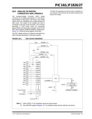
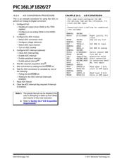
16.2.6 A/D CONVERSION PROCEDURE
This is an example procedure for using the ADC to
perform an Analog-to-Digital conversion:
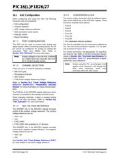
1. Configure Port:
• Disable pin output driver (Refer to the TRIS
register)
• Configure pin as analog (Refer to the ANSEL
register)
2. Configure the ADC module:
• Select ADC conversion clock
• Configure voltage reference
• Select ADC input channel
• Turn on ADC module
3. Configure ADC interrupt (optional):
• Clear ADC interrupt flag
• Enable ADC interrupt
• Enable peripheral interrupt
• Enable global interrupt
(1)
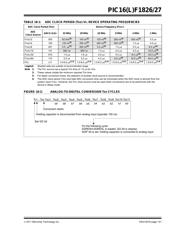
4. Wait the required acquisition time
(2)
.
5. Start conversion by setting the GO/DONE bit.
6. Wait for ADC conversion to complete by one of
the following:
• Polling the GO/DONE
bit
• Waiting for the ADC interrupt (interrupts
enabled)
7. Read ADC Result.
8. Clear the ADC interrupt flag (required if interrupt
is enabled).
EXAMPLE 16-1: A/D CONVERSION
Note 1: The global interrupt can be disabled if the
user is attempting to wake-up from Sleep
and resume in-line code execution.
2: Refer to Section 16.4 “A/D Acquisition
Requirements”.
;This code block configures the ADC
;for polling, Vdd and Vss references, Frc
;clock and AN0 input.
;
;Conversion start & polling for completion
; are included.
;
BANKSEL ADCON1 ;
MOVLW B’11110000’ ;Right justify, Frc
;clock
MOVWF ADCON1 ;Vdd and Vss Vref
BANKSEL TRISA ;
BSF TRISA,0 ;Set RA0 to input
BANKSEL ANSEL ;
BSF ANSEL,0 ;Set RA0 to analog
BANKSEL ADCON0 ;
MOVLW B’00000001’ ;Select channel AN0
MOVWF ADCON0 ;Turn ADC On
CALL SampleTime ;Acquisiton delay
BSF ADCON0,ADGO ;Start conversion
BTFSC ADCON0,ADGO ;Is conversion done?
GOTO $-1 ;No, test again
BANKSEL ADRESH ;
MOVF ADRESH,W ;Read upper 2 bits
MOVWF RESULTHI ;store in GPR space
BANKSEL ADRESL ;
MOVF ADRESL,W ;Read lower 8 bits
MOVWF RESULTLO ;Store in GPR space
器件 Datasheet 文档搜索
AiEMA 数据库涵盖高达 72,405,303 个元件的数据手册,每天更新 5,000 多个 PDF 文件
