Datasheet 搜索 > Microchip(微芯) > PIC16F1827T-E/SS 数据手册 > PIC16F1827T-E/SS 数据手册 208/406 页
 器件3D模型
¥ 0
PIC16F1827T-E/SS 数据手册 - Microchip(微芯)
制造商:
Microchip(微芯)
封装:
SSOP-20
描述:
18 /20/ 28引脚闪存单片机采用纳瓦XLP技术 18/20/28-Pin Flash Microcontrollers with nanoWatt XLP Technology
Pictures:
3D模型
符号图
焊盘图
引脚图
产品图
页面导航:
引脚图在P6P11P12P13P14P131P204P206P213P322Hot
典型应用电路图在P137P323
原理图在P10P16P52P63P73P97P131P135P139P154P158P164
封装尺寸在P384
标记信息在P383
封装信息在P383P385P386P390P391
功能描述在P315
技术参数、封装参数在P54P58P84P98P102P135P140P146P150P153P167P168
应用领域在P47P54P55P215P222
电气规格在P54P58P84P98P135P140P146P150P153P167P169P175
导航目录
PIC16F1827T-E/SS数据手册
Page:
of 406 Go
若手册格式错乱,请下载阅览PDF原文件
PIC16(L)F1826/27
DS41391D-page 208 2011 Microchip Technology Inc.
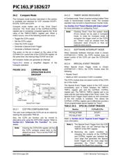
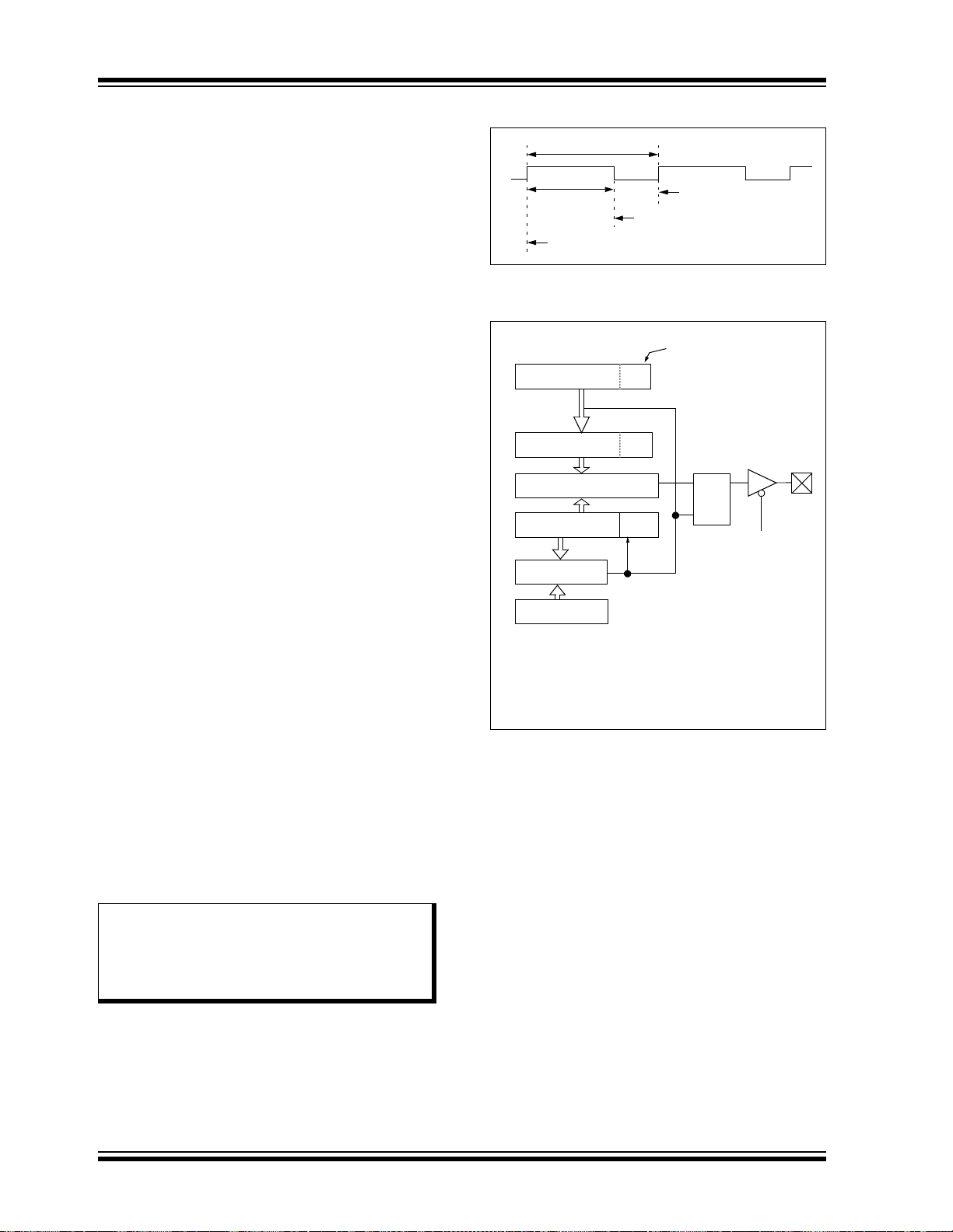
24.3 PWM Overview
Pulse-Width Modulation (PWM) is a scheme that
provides power to a load by switching quickly between
fully on and fully off states. The PWM signal resembles
a square wave where the high portion of the signal is
considered the on state and the low portion of the signal
is considered the off state. The high portion, also known
as the pulse width, can vary in time and is defined in
steps. A larger number of steps applied, which
lengthens the pulse width, also supplies more power to
the load. Lowering the number of steps applied, which
shortens the pulse width, supplies less power. The
PWM period is defined as the duration of one complete
cycle or the total amount of on and off time combined.
PWM resolution defines the maximum number of steps
that can be present in a single PWM period. A higher
resolution allows for more precise control of the pulse
width time and in turn the power that is applied to the
load.
The term duty cycle describes the proportion of the on
time to the off time and is expressed in percentages,
where 0% is fully off and 100% is fully on. A lower duty
cycle corresponds to less power applied and a higher
duty cycle corresponds to more power applied.
Figure 24-3 shows a typical waveform of the PWM
signal.
24.3.1 STANDARD PWM OPERATION
The standard PWM function described in this section is
available and identical for CCP modules ECCP1,
ECCP2, CCP3 and CCP4.
The standard PWM mode generates a Pulse-Width
Modulation (PWM) signal on the CCPx pin with up to 10
bits of resolution. The period, duty cycle, and resolution
are controlled by the following registers:
•PRx registers
•TxCON registers
• CCPRxL registers
• CCPxCON registers
Figure 24-4 shows a simplified block diagram of PWM
operation.
FIGURE 24-3: CCP PWM OUTPUT SIGNAL
FIGURE 24-4: SIMPLIFIED PWM BLOCK
DIAGRAM
Note 1: The corresponding TRIS bit must be
cleared to enable the PWM output on the
CCPx pin.
2: Clearing the CCPxCON register will
relinquish control of the CCPx pin.
Period
Pulse Width
TMRx = 0
TMRx = CCPRxH:CCPxCON<5:4>
TMRx = PRx
CCPRxL
CCPRxH
(2)
(Slave)
Comparator
TMRx
PRx
(1)
RQ
S
Duty Cycle Registers
CCPxCON<5:4>
Clear Timer,
toggle CCPx pin and
latch duty cycle
Note 1: The 8-bit timer TMRx register is concatenated
with the 2-bit internal system clock (F
OSC), or
2 bits of the prescaler, to create the 10-bit time
base.
2: In PWM mode, CCPRxH is a read-only register.
TRIS
CCPx
Comparator
器件 Datasheet 文档搜索
AiEMA 数据库涵盖高达 72,405,303 个元件的数据手册,每天更新 5,000 多个 PDF 文件
