Datasheet 搜索 > 微控制器 > Microchip(微芯) > PIC18F4685-E/ML 数据手册 > PIC18F4685-E/ML 数据手册 146/484 页

 器件3D模型
¥ 34.818
PIC18F4685-E/ML 数据手册 - Microchip(微芯)
制造商:
Microchip(微芯)
分类:
微控制器
封装:
QFN-44
描述:
PIC18 系列 3328 B RAM 96 kB 闪存 8位 微控制器 - QFN-44
Pictures:
3D模型
符号图
焊盘图
引脚图
产品图
页面导航:
引脚图在P4P5P167P169P176Hot
典型应用电路图在P193
原理图在P10P12P13P27P43P146P150P154P160P162P168P169
封装尺寸在P459
标记信息在P457P458
封装信息在P457P459P460P461P462P463
技术参数、封装参数在P432P433P434P436P437P438
应用领域在P180P272
电气规格在P107P260P261P265P266


导航目录
PIC18F4685-E/ML数据手册
Page:
of 484 Go
若手册格式错乱,请下载阅览PDF原文件
PIC18F2682/2685/4682/4685
DS39761B-page 144 Preliminary © 2007 Microchip Technology Inc.
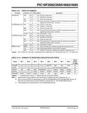
10.6 Parallel Slave Port
In addition to its function as a general I/O port, PORTD
can also operate as an 8-bit wide Parallel Slave Port
(PSP) or microprocessor port. PSP operation is
controlled by the 4 upper bits of the TRISE register
(Register 10-1). Setting control bit, PSPMODE
(TRISE<4>), enables PSP operation, as long as the
Enhanced CCP1 (ECCP1) module is not operating in
dual output or quad output PWM mode. In Slave mode,
the port is asynchronously readable and writable by the
external world.
The PSP can directly interface to an 8-bit micro-
processor data bus. The external microprocessor can
read or write the PORTD latch as an 8-bit latch. Setting
the control bit, PSPMODE, enables the PORTE I/O
pins to become control inputs for the microprocessor
port. When set, port pin RE0 is the RD
input, RE1 is the
WR
input and RE2 is the CS (Chip Select) input. For
this functionality, the corresponding data direction bits
of the TRISE register (TRISE<2:0>) must be config-
ured as inputs (set). The A/D port configuration bits,
PFCG3:PFCG0 (ADCON1<3:0>), must also be set to
‘1010’.
A write to the PSP occurs when both the CS
and WR
lines are first detected low and ends when either are
detected high. The PSPIF and IBF flag bits are both set
when the write ends.
A read from the PSP occurs when both the CS
and RD
lines are first detected low. The data in PORTD is read
out and the OBF bit is set. If the user writes new data
to PORTD to set OBF, the data is immediately read out;
however, the OBF bit is not set.
When either the CS
or RD line is detected high, the
PORTD pins return to the input state and the PSPIF bit
is set. User applications should wait for PSPIF to be set
before servicing the PSP. When this happens, the IBF
and OBF bits can be polled and the appropriate action
taken.
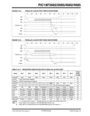
The timing for the control signals in Write and Read
modes is shown in Figure 10-3 and Figure 10-4,
respectively.
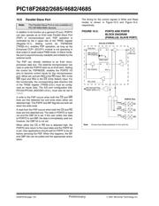
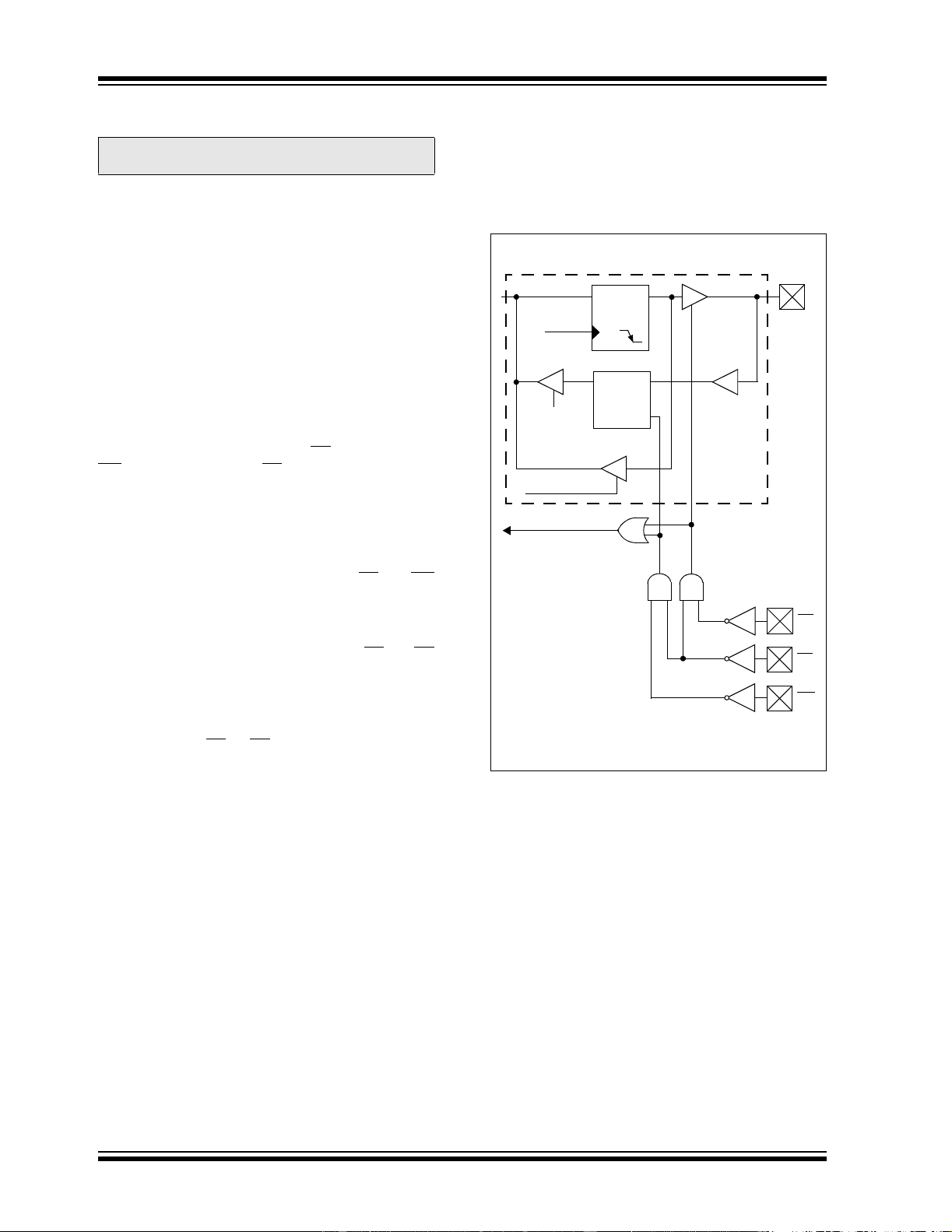
FIGURE 10-2: PORTD AND PORTE
BLOCK DIAGRAM
(PARALLEL SLAVE PORT)
Note: The Parallel Slave Port is only available on
PIC18F4682/4685 devices.
Data Bus
WR LATD or
RDx pin
QD
CK
EN
QD
EN
RD PORTD
One bit of PORTD
Set Interrupt Flag
PSPIF (PIR1<7>)
Read
Chip
Write
RD
CS
WR
TTL
TTL
TTL
TTL
WR PORTD
RD LATD
Data Latch
Note: I/O pins have diode protection to VDD and VSS.
PORTE Pins
Select
器件 Datasheet 文档搜索
AiEMA 数据库涵盖高达 72,405,303 个元件的数据手册,每天更新 5,000 多个 PDF 文件
