Datasheet 搜索 > 微控制器 > Microchip(微芯) > PIC18F97J94-I/PT 数据手册 > PIC18F97J94-I/PT 数据手册 264/696 页
 器件3D模型
¥ 41.077
PIC18F97J94-I/PT 数据手册 - Microchip(微芯)
制造商:
Microchip(微芯)
分类:
微控制器
封装:
TQFP-100
描述:
MICROCHIP PIC18F97J94-I/PT 微控制器, 8位, 闪存, PIC18FxxJxx, 64 MHz, 128 KB, 3.7714 KB, 100 引脚, TQFP
Pictures:
3D模型
符号图
焊盘图
引脚图
产品图
页面导航:
引脚图在P3P4P5P32P40P264P321P322P324P344P346Hot
典型应用电路图在P357P521
原理图在P11P14P15P16P53P60P85P221P236P245P255P282
封装尺寸在P665
标记信息在P663
封装信息在P663P665P666P667P669P671P673P675
功能描述在P489
技术参数、封装参数在P76P488P551P636P637P638P639P641P642P643
应用领域在P62P72P76P326P333P505
电气规格在P11P33P49P76P90P92P461P485P488P492P497P499
导航目录
PIC18F97J94-I/PT数据手册
Page:
of 696 Go
若手册格式错乱,请下载阅览PDF原文件
PIC18F97J94 FAMILY
DS30575A-page 264 2012 Microchip Technology Inc.
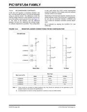
13.8 LCD Multiplex Types
The LCD driver module can be configured into four
multiplex types:
• Static (only COM0 used)
• 1/2 multiplex (COM0 and COM1 are used)
• 1/3 multiplex (COM0, COM1 and COM2 are used)
• 1/4 multiplex (COM0, COM1, COM2 and COM3
are used)
• 1/5 multiplex (COM0, COM1, COM2, COM3 and
COM4 are used)
• 1/6 multiplex (COM0, COM1, COM2, COM3,
COM4 and COM5 are used)
• 1/7 multiplex (COM0, COM1, COM2, COM3,
COM4, COM5 and COM6 are used)
• 1/8 multiplex (COM0, COM1, COM2, COM3,
COM4, COM5, COM6 and COM7 are used)
The LMUX<2:0> setting (LCDCON<2:0>) decides the
function of the COM pins. (For details, see Table 1 3 -4).
If the pin is a digital I/O, the corresponding TRIS bit
controls the data direction. If the pin is a COM drive, the
TRIS setting of that pin is overridden.
13.9 Segment Enables
The LCDSEx registers are used to select the pin function
for each segment pin. The selection allows each pin to
operate as either an LCD segment driver or a digital only
pin. To configure the pin as a segment pin, the corre-
sponding bits in the LCDSEx registers must be set to ‘1’.
If the pin is a digital I/O, the corresponding TRIS bit
controls the data direction. Any bit set in the LCDSEx
registers overrides any bit settings in the corresponding
TRIS register.
13.10 Pixel Control
The LCDDATAx registers contain bits that define the
state of each pixel. Each bit defines one unique pixel.
Table 13-2 shows the correlation of each bit in the
LCDDATAx registers to the respective common and
segment signals.
Any LCD pixel location not being used for display can
be used as general purpose RAM.
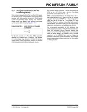
13.11 LCD Frame Frequency
The rate at which the COM and SEG outputs change is
called the LCD frame frequency.
Note: On a Power-on Reset, the LMUX<2:0>
bits are ‘000’.
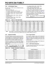
TABLE 13-4: COM<7:0> PIN FUNCTIONS
LMUX<2:0> COM7 Pin COM6 Pin COM5 Pin COM4 Pin COM3 Pin COM2 Pin COM1 Pin COM0 Pin
111 COM7 COM6 COM5 COM4 COM3 COM2 COM1 COM0
110 I/O Pin COM6 COM5 COM4 COM3 COM2 COM1 COM0
101 I/O Pin I/O Pin COM5 COM4 COM3 COM2 COM1 COM0
100 I/O Pin I/O Pin I/O Pin COM4 COM3 COM2 COM1 COM0
011 I/O Pin I/O Pin I/O Pin I/O Pin COM3 COM2 COM1 COM0
010 I/O Pin I/O Pin I/O Pin I/O Pin I/O Pin COM2 COM1 COM0
001 I/O Pin I/O Pin I/O Pin I/O Pin I/O Pin I/O Pin COM1 COM0
000 I/O Pin I/O Pin I/O Pin I/O Pin I/O Pin I/O Pin I/O Pin COM0
Note: Pins, COM<7:4>, can also be used as SEG pins when ¼ multiplex to static multiplex are used. These pins
can be used as I/O pins only if respective bits in the LCDSEx registers are set to ‘0’.
Note: On a Power-on Reset, these pins are
configured as digital I/O.
TABLE 13-5: FRAME FREQUENCY FORMULAS
Multiplex Frame Frequency =
Static (‘000’) Clock Source/(4 x 1 x (LP<3:0> + 1))
1/2 (‘001’) Clock Source/(2 x 2 x (LP<3:0> + 1))
1/3 (‘010’) Clock Source/(1 x 3 x (LP<3:0> + 1))
1/4 (‘011’) Clock Source/(1 x 4 x (LP<3:0> + 1))
1/5 (‘100’) Clock Source/(1 x 5 x (LP<3:0> + 1))
1/6 (‘101’) Clock Source/(1 x 6 x (LP<3:0> + 1))
1/7 (‘110’) Clock Source/(1 x 7 x (LP<3:0> + 1))
1/8 (‘111’) Clock Source/(1 x 8 x (LP<3:0> + 1))
Note: The clock source is FRC/8192, SOSC/32 or LPRC/32.
器件 Datasheet 文档搜索
AiEMA 数据库涵盖高达 72,405,303 个元件的数据手册,每天更新 5,000 多个 PDF 文件
