Datasheet 搜索 > 微控制器 > Microchip(微芯) > PIC18F97J94-I/PT 数据手册 > PIC18F97J94-I/PT 数据手册 282/696 页
 器件3D模型
¥ 41.077
PIC18F97J94-I/PT 数据手册 - Microchip(微芯)
制造商:
Microchip(微芯)
分类:
微控制器
封装:
TQFP-100
描述:
MICROCHIP PIC18F97J94-I/PT 微控制器, 8位, 闪存, PIC18FxxJxx, 64 MHz, 128 KB, 3.7714 KB, 100 引脚, TQFP
Pictures:
3D模型
符号图
焊盘图
引脚图
产品图
页面导航:
引脚图在P3P4P5P32P40P264P321P322P324P344P346Hot
典型应用电路图在P357P521
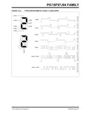
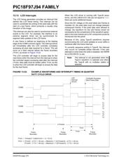
原理图在P11P14P15P16P53P60P85P221P236P245P255P282
封装尺寸在P665
标记信息在P663
封装信息在P663P665P666P667P669P671P673P675
功能描述在P489
技术参数、封装参数在P76P488P551P636P637P638P639P641P642P643
应用领域在P62P72P76P326P333P505
电气规格在P11P33P49P76P90P92P461P485P488P492P497P499
导航目录
PIC18F97J94-I/PT数据手册
Page:
of 696 Go
若手册格式错乱,请下载阅览PDF原文件
PIC18F97J94 FAMILY
DS30575A-page 282 2012 Microchip Technology Inc.
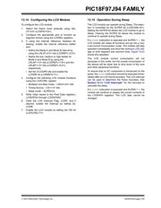
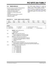
14.1 Timer0 Operation
Timer0 can operate in one of these two modes:
• As an 8-bit (T08BIT = 1) or 16-bit (T08BIT = 0)
timer
• As an asynchronous 8-bit (T08BIT = 1) or 16-bit
(T08BIT = 0) counter
14.1.1 TIMER MODE
In Timer mode, Timer0 either increments every CPU
clock cycle, or every instruction cycle, depending on
the clock select bit, TMR0CS<1:0> (T0CON<7:6>).
14.1.2 COUNTER MODE
In this mode, Timer0 is incremented via a rising or fall-
ing edge of an external source on the T0CKI pin. The
clock select bits, TMR0CS<1:0>, must be set to ‘1x’.
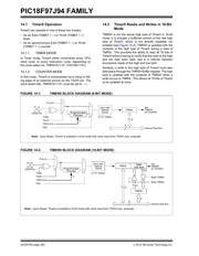
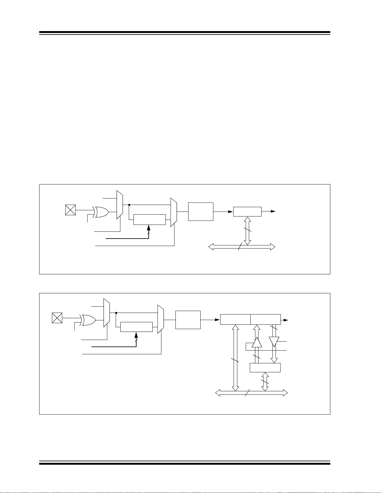
14.2 Timer0 Reads and Writes in 16-Bit
Mode
TMR0H is not the actual high byte of Timer0 in 16-bit
mode. It is actually a buffered version of the real high
byte of Timer0, which is not directly readable nor
writable (see Figure 14-2). TMR0H is updated with the
contents of the high byte of Timer0 during a read of
TMR0L. This provides the ability to read all 16 bits of
Timer0 without having to verify that the read of the high
and low byte were valid, due to a rollover between
successive reads of the high and low byte.
Similarly, a write to the high byte of Timer0 must also
take place through the TMR0H Buffer register. The high
byte is updated with the contents of TMR0H when a
write occurs to TMR0L. This allows all 16 bits of Timer0
to be updated at once.
FIGURE 14-1: TIMER0 BLOCK DIAGRAM (8-BIT MODE)
FIGURE 14-2: TIMER0 BLOCK DIAGRAM (16-BIT MODE)
Note: Upon Reset, Timer0 is enabled in 8-bit mode with clock input from T0CKI max. prescale.
T0CKI Pin
T0SE
0
1
1
0
T0CS
FOSC/4
Sync with
Internal
Clocks
TMR0L
(2 TCY Delay)
Internal Data Bus
PSA
T0PS<2:0>
Set
TMR0IF
on Overflow
3
8
8
Programmable
Prescaler
Note: Upon Reset, Timer0 is enabled in 8-bit mode with clock input from T0CKI max. prescale.
T0CKI Pin
T0SE
0
1
1
0
T0CS
FOSC/4
Sync with
Internal
Clocks
TMR0L
(2 TCY Delay)
Internal Data Bus
8
PSA
T0PS<2:0>
Set
TMR0IF
on Overflow
3
TMR0
TMR0H
High Byte
8
8
8
Read TMR0L
Write TMR0L
8
Programmable
Prescaler
器件 Datasheet 文档搜索
AiEMA 数据库涵盖高达 72,405,303 个元件的数据手册,每天更新 5,000 多个 PDF 文件
