Datasheet 搜索 > 微控制器 > Renesas Electronics(瑞萨电子) > R5F52105BDFN#V0 数据手册 > R5F52105BDFN#V0 数据手册 1/164 页
 器件3D模型
¥ 88.777
R5F52105BDFN#V0 数据手册 - Renesas Electronics(瑞萨电子)
制造商:
Renesas Electronics(瑞萨电子)
分类:
微控制器
封装:
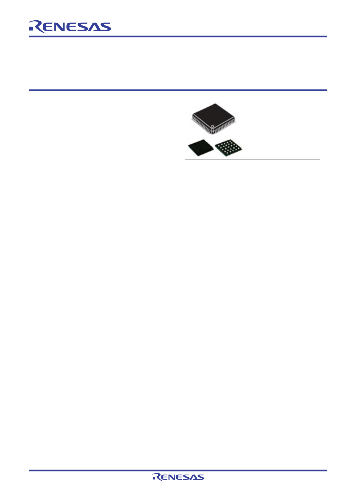
LQFP
描述:
RX210 微控制器RX210 低功率微控制器具有宽工作范围并且可以在高达 50 MHz 78 DMIPS 时执行计算。 使用 RX210 的应用包括数码相机、洗衣机、功率计、智能手机、医疗保健设备和冰箱。工作范围:1.62 V 至 5.3 V 事件链接控制器 (ELC) 多功能引脚控制器 (MPC) 三相电动机控制计时器 (MTU2) 12 位模/数转换器 4 种功耗模式: -睡眠模式 -所有模块时钟停止模式 -软件待机模式 -深度软件待机模式 ### RX 系列微控制器,Renesas ElectronicsRX 系列 32 位闪存微控制器持续发展,用于工业、消费品和办公自动化应用。
Pictures:
3D模型
符号图
焊盘图
引脚图
产品图
页面导航:
引脚图在P13P14P15P16P17P18P19P20P21P22P23P24Hot
原理图在P12
封装尺寸在P17P153P154P155P156P157P158P159P160P161
功能描述在P2P3P4P5
技术参数、封装参数在P2P3P4P5P64
电气规格在P64P65P66P67P68P69P70P71P72P73P74P75
导航目录
R5F52105BDFN#V0数据手册
Page:
of 164 Go
若手册格式错乱,请下载阅览PDF原文件
Datasheet
R01DS0041EJ0120 Rev.1.20 Page 1 of 162
Nov 28, 2012
RX210 Group
Renesas MCUs
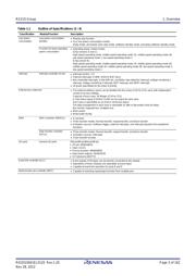
Features
■ 32-bit RX CPU core
Max. operating frequency: 50 MHz
Capable of 78 DMIPS in operation at 50 MHz
Accumulator handles 64-bit results (for a single
instruction) from 32- × 32-bit operations
Multiplication and division unit handles 32- × 32-bit
operations (multiplication instructions take one CPU
clock cycle)
Fast interrupt
CISC Harvard architecture with 5-stage pipeline
Variable-length instructions, ultra-compact code
On-chip debugging circuit
■ Low power design and architecture
Operation from a single 1.62-V to 5.5-V supply
1.62-V operation available (at up to 20 MHz)
Deep software standby mode with RTC remaining usable
Four low power modes
■ On-chip flash memory for code, no wait states
50-MHz operation, 20-ns read cycle
No wait states for reading at full CPU speed
64-K to 512-Kbyte capacities
User code programmable via the SCI
Programmable at 1.62 V
For instructions and operands
■ On-chip data flash memory
8 Kbytes
(Number of times of reprogramming: 100,000)
Erasing and programming impose no load on the CPU.
■ On-chip SRAM, no wait states
12-K to 64-Kbyte size capacities
■ DMA
DMAC: Incorporates four channels
DTC: Four transfer modes
■ ELC
Module operation can be initiated by event signals
without going through interrupts.
Modules can operate while the CPU is sleeping.
■ Reset and supply management
Nine types of reset, including the power-on reset (POR)
Low voltage detection (LVD) with voltage settings
■ Clock functions
Frequency of external clock: Up to 20 MHz
Frequency of the oscillator for sub-clock generation:
32.768 kHz
PLL circuit input: 4 MHz to 12.5 MHz
On-chip low- and high-speed oscillators, dedicated on-
chip low-speed oscillator for the IWDT
Generation of a dedicated 32.768-kHz clock for the RTC
Clock frequency accuracy measurement circuit (CAC)
■
Real-time clock
Adjustment fu
nctions (30 seconds, leap year, and error)
Time capture functio
n
Time capture on event-signal input through external pins
RTC capable of initiating return from deep software
standby mode
■ Independent watchdog timer
125-kHz on-chip oscillator produces a dedicated clock
signal to drive IWDT operation.
■ Useful functions for IEC60730 compliance
Self-diagnostic and disconnection-detection assistance
functions for the A/D converter, clock frequency
accuracy measurement circuit, independent watchdog
timer, functions to assist in RAM testing, etc.
■ Up to nine communications channels
SCI with many useful functions (up to seven channels)
Asynchronous mode, clock synchronous mode, smart
card interface
I
2
C bus interface: Transfer at up to 400 kbps, capable of
SMBus operation (one channel)
RSPI (one channel)
■ External address space
Four CS areas (4 × 16 Mbytes)
8- or 16-bit bus space is selectable per area
■ Up to 14 extended-function timers
16-bit MTU: input capture, output compare,
complementary PWM output, phase counting mode
(six channels)
8-bit TMR (four channels)
16-bit compare-match timers (four channels)
■ 12-bit A/D converter
Capable of conversion within 1 μs
Sample-and-hold circuits (for three channels)
Three-channel synchronized sampling available
Self-diagnostic function and analog input disconnection
detection assistance function
■ 10-bit D/A converter
■ Analog comparator
■ General I/O ports
5-V tolerant, open drain, input pull-up, switching of
driving ability
■ MPC
Multiple locations are selectable for I/O pins of
peripheral functions
■ Temperature sensor
■ Operating temp. range
40C to +85C
40C to +105C
PLQP0100KB-A 14 × 14 mm, 0.5-mm pitch
PLQP0080KB-A 12 × 12 mm, 0.5-mm pitch
PLQP0064KB-A 10 × 10 mm, 0.5-mm pitch
PLQP0048KB-A 7 × 7 mm, 0.5-mm pitch
PLQP0080JA-A 14 × 14 mm, 0.65-mm pitch
PLQP0064GA-A 14 × 14 mm, 0.8-mm pitch
PTLG0100JA-A 7 × 7 mm, 0.65-mm pitch
PTLG0100KA-A 5.5 × 5.5 mm, 0.5-mm pitch
PTLG0064JA-A 6 × 6 mm, 0.65-mm pitch
50-MHz 32-bit RX MCUs, 78 DMIPS, up to 512-KB flash memory,
12-bit A/D, 10-bit D/A, ELC, MPC, RTC, up to 9 comms channels;
incorporating functions for IEC60730 compliance
R01DS0041EJ0120
Rev.1.20
Nov 28, 2012
器件 Datasheet 文档搜索
AiEMA 数据库涵盖高达 72,405,303 个元件的数据手册,每天更新 5,000 多个 PDF 文件
