Datasheet 搜索 > 微控制器 > Renesas Electronics(瑞萨电子) > R5F52105BDFN#V0 数据手册 > R5F52105BDFN#V0 数据手册 13/164 页
 器件3D模型
¥ 88.786
R5F52105BDFN#V0 数据手册 - Renesas Electronics(瑞萨电子)
制造商:
Renesas Electronics(瑞萨电子)
分类:
微控制器
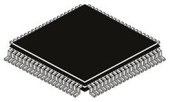
封装:
LQFP
描述:
RX210 微控制器RX210 低功率微控制器具有宽工作范围并且可以在高达 50 MHz 78 DMIPS 时执行计算。 使用 RX210 的应用包括数码相机、洗衣机、功率计、智能手机、医疗保健设备和冰箱。工作范围:1.62 V 至 5.3 V 事件链接控制器 (ELC) 多功能引脚控制器 (MPC) 三相电动机控制计时器 (MTU2) 12 位模/数转换器 4 种功耗模式: -睡眠模式 -所有模块时钟停止模式 -软件待机模式 -深度软件待机模式 ### RX 系列微控制器,Renesas ElectronicsRX 系列 32 位闪存微控制器持续发展,用于工业、消费品和办公自动化应用。
Pictures:
3D模型
符号图
焊盘图
引脚图
产品图
页面导航:
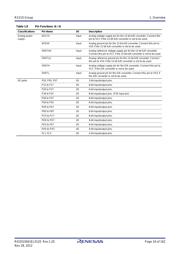
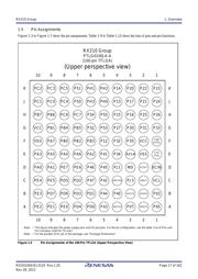
引脚图在P13P14P15P16P17P18P19P20P21P22P23P24Hot
原理图在P12
封装尺寸在P17P153P154P155P156P157P158P159P160P161
功能描述在P2P3P4P5
技术参数、封装参数在P2P3P4P5P64
电气规格在P64P65P66P67P68P69P70P71P72P73P74P75
导航目录
R5F52105BDFN#V0数据手册
Page:
of 164 Go
若手册格式错乱,请下载阅览PDF原文件
R01DS0041EJ0120 Rev.1.20 Page 13 of 162
Nov 28, 2012
RX210 Group 1. Overview
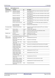
1.4 Pin Functions
Table 1.8 lists the pin functions.
Table 1.8 Pin Functions (1 / 4)
Classifications Pin Name I/O Description
Power supply VCC Input Power supply pin. Connect it to the system power supply.
VCL — Connect this pin to the VSS pin via the 0.1 μF smoothing capacitor
used to stabilize the internal power supply. Place the capacitor close
to the pin.
VSS Input Ground pin. Connect it to the system power supply (0 V).
Clock XTAL Output Pins for connecting a crystal resonator. An external clock signal can
be input through the EXTAL pin.
EXTAL Input
BCLK Output Outputs the external bus clock for external devices.
XCIN Input Input/output pins for the sub-clock oscillator. Connect a crystal
resonator between XCIN and XCOUT.
XCOUT Output
Operating mode
control
MD Input Pin for setting the operating mode. The signal levels on this pin
must not be changed during operation.
System control RES# Input Reset pin. This LSI enters the reset state when this signal goes low.
CAC CACREF Input Input pin for the measuring circuit for clock frequency precision.
On-chip emulator FINED I/O FINE interface pin.
Address bus A0 to A23 Output Output pins for the address.
Data bus D0 to D15 I/O Input and output pins for the bidirectional data bus.
Multiplexed bus A0/D0 to A15/D15 I/O Address/data multiplexed bus
Bus control RD# Output Strobe signal which indicates that reading from the external bus
interface space is in progress.
WR# Output Strobe signal which indicates that writing to the external bus
interface space is in progress, in single-write strobe mode.
WR0#, WR1# Output Strobe signals which indicate that either group of data bus pins (D7
to D0, and D15 to D8) is valid in writing to the external bus interface
space, in byte strobe mode.
BC0#, BC1# Output Strobe signals which indicate that either group of data bus pins (D7
to D0 and D15 to D8) is valid in access to the external bus interface
space, in single-write strobe mode.
CS0# to CS3# Output Select signals for areas 0 to 3.
WAIT# Input Input pin for wait request signals in access to the external space.
ALE Output Address latch signal when address/data multiplexed bus is
selected.
Interrupt NMI Input Non-maskable interrupt request pin.
IRQ0 to IRQ7 Input Interrupt request pins.
器件 Datasheet 文档搜索
AiEMA 数据库涵盖高达 72,405,303 个元件的数据手册,每天更新 5,000 多个 PDF 文件
