Datasheet 搜索 > 微控制器 > Renesas Electronics(瑞萨电子) > R5F52105BDLA#U0 数据手册 > R5F52105BDLA#U0 数据手册 3/223 页
¥ 16.527
R5F52105BDLA#U0 数据手册 - Renesas Electronics(瑞萨电子)
制造商:
Renesas Electronics(瑞萨电子)
分类:
微控制器
封装:
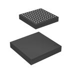
TFLGA-100
描述:
其他系列 50MHz 128K@x8bit
Pictures:
3D模型
符号图
焊盘图
引脚图
产品图
页面导航:
引脚图在P14P15P16P17P18P19P20P21P22P23P24P25Hot
原理图在P13
封装尺寸在P18P20P23P24P207P208P209P210P211P212P213P214
功能描述在P2P3P4P5P6
技术参数、封装参数在P2P3P4P5P6P87
应用领域在P1
电气规格在P87P88P89P90P91P92P93P94P95P96P97P98
导航目录
R5F52105BDLA#U0数据手册
Page:
of 223 Go
若手册格式错乱,请下载阅览PDF原文件

R01DS0041EJ0150 Rev.1.50 Page 3 of 221
Oct 18, 2013
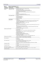
RX210 Group 1. Overview
Low power
consumption
Low power consumption
facilities
Module stop function
Four low power consumption modes
Sleep mode, all-module clock stop mode, software standby mode, and deep software standby mode
Function for lower operating
power consumption
Operating power control modes
[Chip versions A and C]
High-speed operating mode, middle-speed operating mode 1A, middle-speed operating mode 1B,
low-speed operating mode 1, low-speed operating mode 2
[Chip version B]
High-speed operating mode, middle-speed operating mode 1A, middle-speed operating mode 1B,
middle-speed operating mode 2A, middle-speed operating mode 2B, low-speed operating mode 1,
low-speed operating mode 2
Interrupt Interrupt controller (ICUb)
Interrupt vectors: 167
External interrupts: 9 (NMI, IRQ0 to IRQ7 pins)
Non-maskable interrupts: 6 (the NMI pin, oscillation stop detection interrupt, voltage monitoring 1
interrupt, voltage monitoring 2 interrupt, WDT interrupt, and IWDT interrupt)
16 levels specifiable for the order of priority
External bus extension
The external address space can be divided into four areas (CS0 to CS3), each with independent
control of access settings.
Capacity of each area: 16 Mbytes (CS0 to CS3)
A chip-select signal (CS0# to CS3#) can be output for each area.
Each area is specifiable as an 8-bit or 16-bit bus space
The data arrangement in each area is selectable as little or big endian (only for data).
Bus format: Separate bus, multiplex bus
Wait control
Write buffer facility
DMA DMA controller (DMACA)
4 channels
Three transfer modes: Normal transfer, repeat transfer, and block transfer
Activation sources: Software trigger, external interrupts, and interrupt requests from peripheral
functions
Data transfer controller
(DTCa)
Three transfer modes: Normal transfer, repeat transfer, and block transfer
Activation sources: Interrupts
Chain transfer function
I/O ports General I/O ports 145-pin/144-pin/100-pin/80-pin/69-pin/64-pin/48-pin
I/O: 122/122/84/64/48/48/34
Input: 1/1/1/1/1/1/1
Pull-up resistors: 122/122/84/64/48/48/34
Open-drain outputs: 76/76/54/44/35/35/26
5-V tolerance:4/4/4/4/2/2*
1
/2
Event link controller (ELC)
Event signals of 59 types can be directly connected to the module
Operations of timer modules are selectable at event input
Capable of event link operation for ports B and E
Multi-function pin controller (MPC)
Capable of selecting input/output function from multiple pins
Table 1.1 Outline of Specifications (2 / 5)
Classification Module/Function Description
器件 Datasheet 文档搜索
AiEMA 数据库涵盖高达 72,405,303 个元件的数据手册,每天更新 5,000 多个 PDF 文件

