Datasheet 搜索 > 电压基准芯片 > ADI(亚德诺) > REF198FSZ-REEL 数据手册 > REF198FSZ-REEL 数据手册 6/28 页

 器件3D模型
¥ 2.099
REF198FSZ-REEL 数据手册 - ADI(亚德诺)
制造商:
ADI(亚德诺)
分类:
电压基准芯片
封装:
SOIC-8
描述:
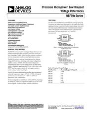
精密微功耗,低压差电压基准 Precision Micropower, Low Dropout Voltage References
Pictures:
3D模型
符号图
焊盘图
引脚图
产品图
页面导航:
引脚图在P1Hot
原理图在P19
封装尺寸在P25
型号编码规则在P26
功能描述在P1
技术参数、封装参数在P1P3P15
应用领域在P1P19P22
电气规格在P3P4P5P6P7P8P9P10P11P12P13P14
导航目录
REF198FSZ-REEL数据手册
Page:
of 28 Go
若手册格式错乱,请下载阅览PDF原文件
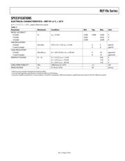
REF19x Series
Rev. I | Page 6 of 28
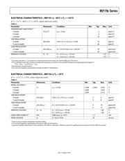
ELECTRICAL CHARACTERISTICS—REF192 @ −40°C ≤ T
A
≤ +85°C
@ V
S
= 3.3 V, −40°C ≤ T
A
≤ +85°C, unless otherwise noted.
Table 6.
Parameter Mnemonic Condition Min Typ Max Unit
TEMPERATURE COEFFICIENT
1, 2
E Grade TCV
O
/°C I
OUT
= 0 mA 2 5 ppm/°C
F Grade 5 10 ppm/°C
G Grade
3
10 25 ppm/°C
LINE REGULATION
4
E Grade ΔV
O
/ΔV
IN
3.0 V ≤ V
S
≤ 15 V, I
OUT
= 0 mA 5 10 ppm/V
F and G Grades 10 20 ppm/V
LOAD REGULATION
4
E Grade ΔV
O
/ΔV
LOAD
V
S
= 5.0 V, 0 mA ≤ I
OUT
≤ 25 mA 5 15 ppm/mA
F and G Grades 10 20 ppm/mA
DROPOUT VOLTAGE V
S
− V
O
V
S
= 3.5 V, I
LOAD
= 10 mA 1.00 V
V
S
= 4.0 V, I
LOAD
= 25 mA 1.50 V
SLEEP
PIN
Logic High Input Voltage V
H
2.4 V
Logic High Input Current I
H
−8 μA
Logic Low Input Voltage V
L
0.8 V
Logic Low Input Current I
L
−8 μA
SUPPLY CURRENT No load 45 μA
Sleep Mode No load 15 μA
1
For proper operation, a 1 μF capacitor is required between the output pin and the GND pin of the device.
2
TCV
O
is defined as the ratio of output change with temperature variation to the specified temperature range expressed in ppm/°C.
TCV
O
= (V
MAX
− V
MIN
)/V
O
(T
MAX
− T
MIN
)
3
Guaranteed by characterization.
4
Line and load regulation specifications include the effect of self-heating.
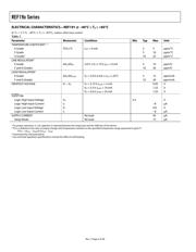
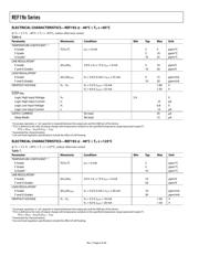
ELECTRICAL CHARACTERISTICS—REF192 @ −40°C ≤ T
A
≤ +125°C
@ V
S
= 3.3 V, −40°C ≤ T
A
≤ +125°C, unless otherwise noted.
Table 7.
Parameter Mnemonic Condition Min Typ Max Unit
TEMPERATURE COEFFICIENT
1, 2
E Grade TCV
O
/°C I
OUT
= 0 mA 2 ppm/°C
F Grade 5 ppm/°C
G Grade
3
10 ppm/°C
LINE REGULATION
4
E Grade ΔV
O
/ΔV
IN
3.0 V ≤ V
S
≤ 15 V, I
OUT
= 0 mA 10 ppm/V
F and G Grades 20 ppm/V
LOAD REGULATION
4
E Grade ΔV
O
/ΔV
LOAD
V
S
= 5.0 V, 0 mA ≤ I
OUT
≤ 20 mA 10 ppm/mA
F and G Grades 20 ppm/mA
DROPOUT VOLTAGE V
S
− V
O
V
S
= 3.5 V, I
LOAD
= 10 mA 1.00 V
V
S
= 4.0 V, I
LOAD
= 20 mA 1.50 V
1
For proper operation, a 1 μF capacitor is required between the output pin and the GND pin of the device.
2
TCV
O
is defined as the ratio of output change with temperature variation to the specified temperature range expressed in ppm/°C.
TCV
O
= (V
MAX
− V
MIN
)/V
O
(T
MAX
− T
MIN
)
3
Guaranteed by characterization.
4
Line and load regulation specifications include the effect of self-heating.
器件 Datasheet 文档搜索
AiEMA 数据库涵盖高达 72,405,303 个元件的数据手册,每天更新 5,000 多个 PDF 文件
