Datasheet 搜索 > 开发套件与开发板 > Silicon Labs(芯科) > SI4735-D60-EVB 数据手册 > SI4735-D60-EVB 数据手册 7/42 页

¥ 1094.685
SI4735-D60-EVB 数据手册 - Silicon Labs(芯科)
制造商:
Silicon Labs(芯科)
分类:
开发套件与开发板
Pictures:
3D模型
符号图
焊盘图
引脚图
产品图
页面导航:
引脚图在P1P29P40Hot
典型应用电路图在P18P19P26P40P42
原理图在P1P12P13P14P15P18P19P21P22P26P39P40
封装尺寸在P32P33
型号编码规则在P1P31
标记信息在P37P38
功能描述在P21P40
技术参数、封装参数在P5P17
应用领域在P1
电气规格在P5
导航目录
SI4735-D60-EVB数据手册
Page:
of 42 Go
若手册格式错乱,请下载阅览PDF原文件
Si4730/31/34/35-D60
Rev. 1.2 7
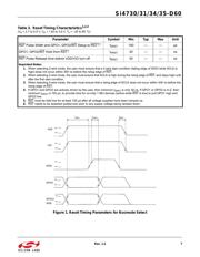
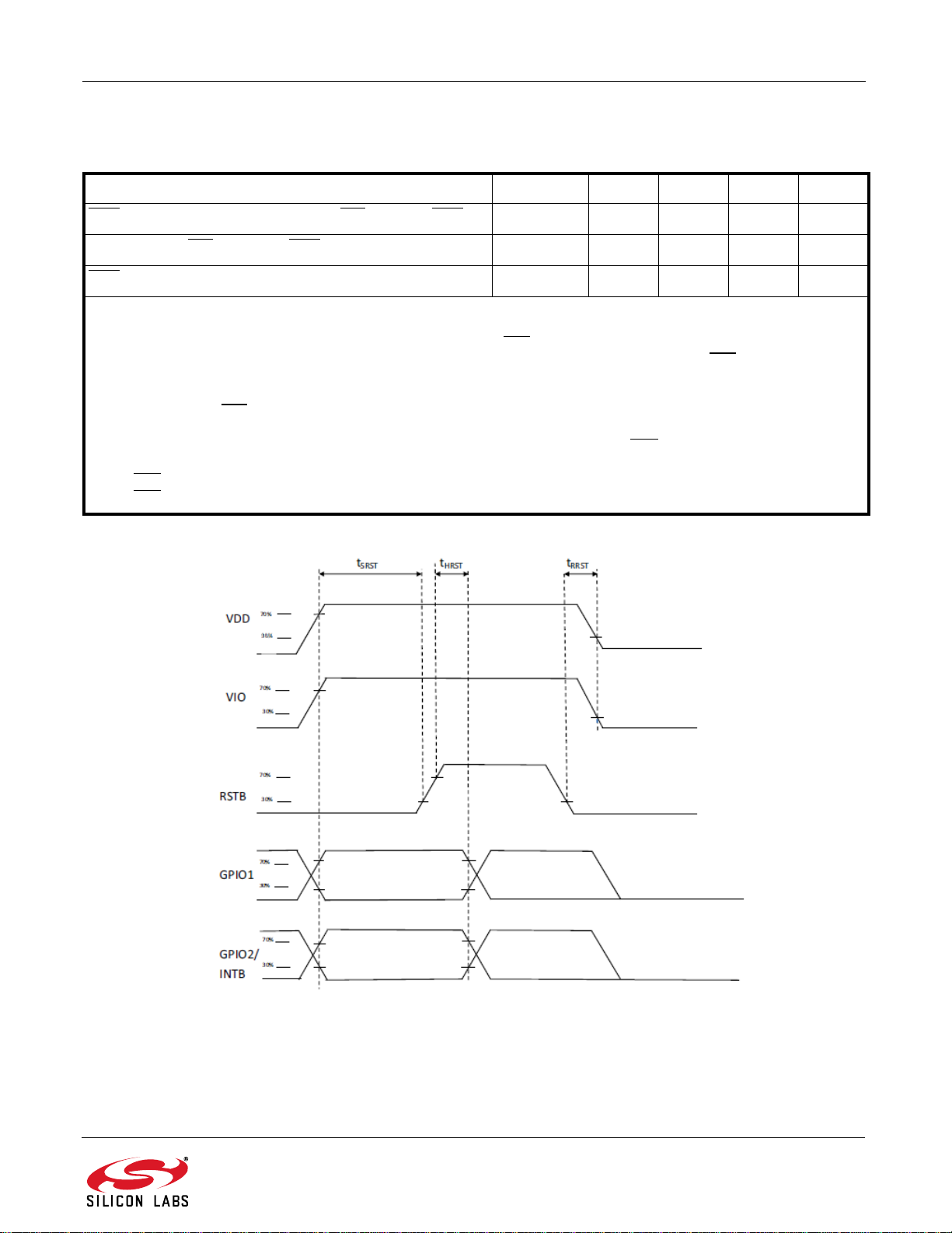
Figure 1. Reset Timing Parameters for Busmode Select
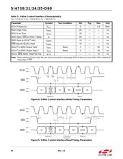
Table 3. Reset Timing Characteristics
1,2,3
(V
A
= 2.7 to 5.5 V, V
D
= 1.62 to 3.6 V, T
A
= –20 to 85 °C)
Parameter Symbol Min Typ Max Unit
RST
Pulse Width and GPO1, GPO2/INT Setup to RST
t
SRST
100 — — µs
GPO1, GPO2/INT
Hold from RST t
HRST
30 — — ns
RST
Pulse Release time before VDD/VIO turn off t
RRST
30 — — ns
Important Notes:
1. When selecting 2-wire mode, the user must ensure that a 2-wire start condition (falling edge of SDIO while SCLK is
high) does not occur within 300 ns before the rising edge of RST
.
2. When selecting 2-wire mode, the user must ensure that SCLK is high during the rising edge of RST, and stays high until
after the first start condition.
3. When selecting 3-wire mode, the user must ensure that a rising edge of SCLK does not occur within 300 ns before the
rising edge of RST
.
4. If GPO1 and GPO2 are actively driven by the user, then minimum t
SRST
is only 30 ns. If GPO1 or GPO2 is hi-Z, then
minimum t
SRST
is 100 µs, to provide time for on-chip 1 M devices (active while RST is low) to pull GPO1 high and
GPO2 low.
5. RST
must be held low for at least 100 µs after all voltage supplies have been ramped up.
6. RST needs to be asserted (pulled low) prior to any supply voltage being ramped down.
器件 Datasheet 文档搜索
AiEMA 数据库涵盖高达 72,405,303 个元件的数据手册,每天更新 5,000 多个 PDF 文件
