Datasheet 搜索 > 电池管理芯片 > TI(德州仪器) > SN6501QDBVRQ1 数据手册 > SN6501QDBVRQ1 数据手册 15/34 页

¥ 7.576
SN6501QDBVRQ1 数据手册 - TI(德州仪器)
制造商:
TI(德州仪器)
分类:
电池管理芯片
封装:
SOT-23-5
描述:
TEXAS INSTRUMENTS SN6501QDBVRQ1 芯片, 变压器驱动器, AEC-Q100, SOT-23-5
Pictures:
3D模型
符号图
焊盘图
引脚图
产品图
页面导航:
引脚图在P3Hot
典型应用电路图在P15P21
原理图在P1P12P14P15
封装尺寸在P28P30P31
标记信息在P28
封装信息在P27P28P29P30P31
技术参数、封装参数在P3P5P6P7P8P9P10
应用领域在P1P34
电气规格在P4
导航目录
SN6501QDBVRQ1数据手册
Page:
of 34 Go
若手册格式错乱,请下载阅览PDF原文件
SN6501-Q1
www.ti.com
SLLSEF3A –JUNE 2013–REVISED SEPTEMBER 2014
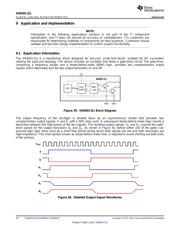
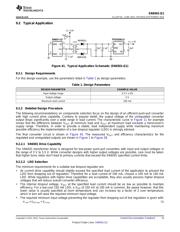
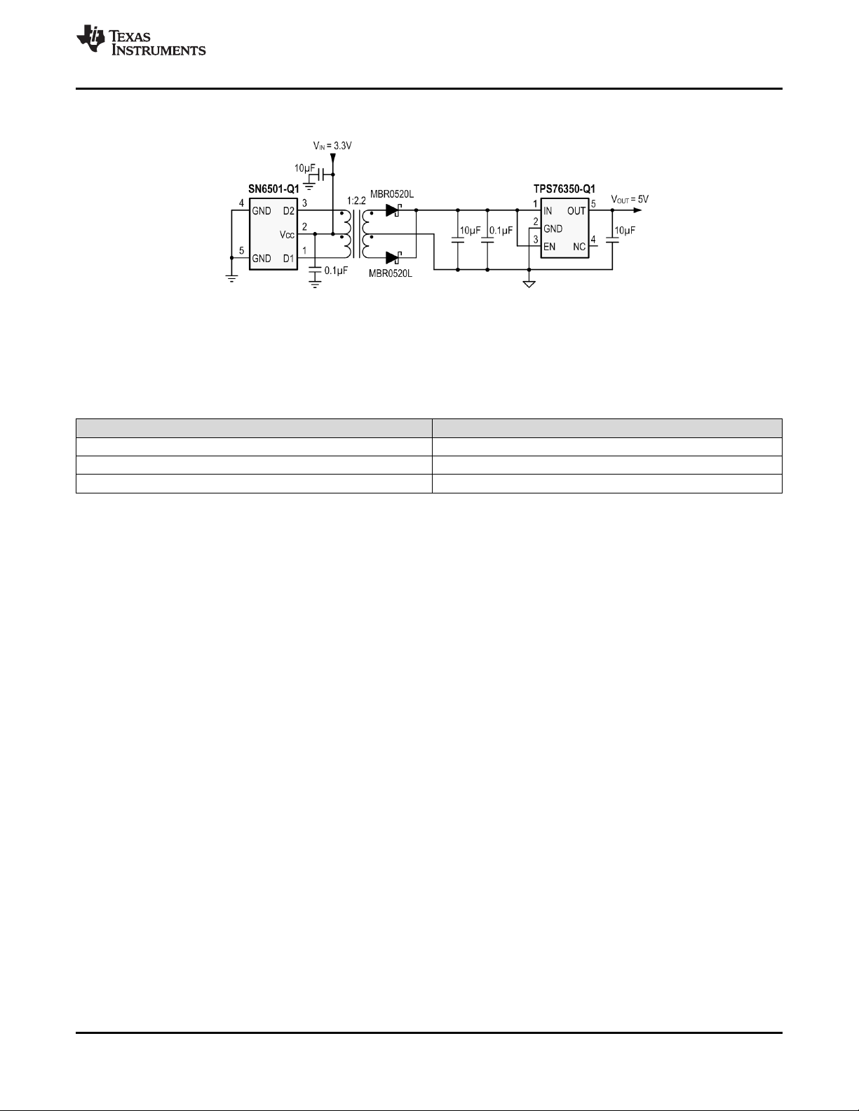
9.2 Typical Application
Figure 41. Typical Application Schematic (SN6501-Q1)
9.2.1 Design Requirements
For this design example, use the parameters listed in Table 1 as design parameters.
Table 1. Design Parameters
DESIGN PARAMETER EXAMPLE VALUE
Input voltage range 3.3 V ± 3%
Output voltage 5 V
Maximum load current 100 mA
9.2.2 Detailed Design Procedure
The following recommendations on components selection focus on the design of an efficient push-pull converter
with high current drive capability. Contrary to popular belief, the output voltage of the unregulated converter
output drops significantly over a wide range in load current. The characteristic curve in Figure 11 for example
shows that the difference between V
OUT
at minimum load and V
OUT
at maximum load exceeds a transceiver’s
supply range. Therefore, in order to provide a stable, load independent supply while maintaining maximum
possible efficiency the implementation of a low dropout regulator (LDO) is strongly advised.
The final converter circuit is shown in Figure 45. The measured V
OUT
and efficiency characteristics for the
regulated and unregulated outputs are shown in Figure 1 to Figure 28.
9.2.2.1 SN6501 Drive Capability
The SN6501 transformer driver is designed for low-power push-pull converters with input and output voltages in
the range of 3 V to 5.5 V. While converter designs with higher output voltages are possible, care must be taken
that higher turns ratios don’t lead to primary currents that exceed the SN6501 specified current limits.
9.2.2.2 LDO Selection
The minimum requirements for a suitable low dropout regulator are:
• Its current drive capability should slightly exceed the specified load current of the application to prevent the
LDO from dropping out of regulation. Therefore for a load current of 100 mA, choose a 100 mA to 150 mA
LDO. While regulators with higher drive capabilities are acceptable, they also usually possess higher dropout
voltages that will reduce overall converter efficiency.
• The internal dropout voltage, V
DO
, at the specified load current should be as low as possible to maintain
efficiency. For a low-cost 150 mA LDO, a V
DO
of 150 mV at 100 mA is common. Be aware however, that this
lower value is usually specified at room temperature and can increase by a factor of 2 over temperature,
which in turn will raise the required minimum input voltage.
• The required minimum input voltage preventing the regulator from dropping out of line regulation is given with:
V
I-min
= V
DO-max
+ V
O-max
(1)
Copyright © 2013–2014, Texas Instruments Incorporated Submit Documentation Feedback 15
Product Folder Links: SN6501-Q1
器件 Datasheet 文档搜索
AiEMA 数据库涵盖高达 72,405,303 个元件的数据手册,每天更新 5,000 多个 PDF 文件
