Datasheet 搜索 > 电池管理芯片 > TI(德州仪器) > SN6501QDBVRQ1 数据手册 > SN6501QDBVRQ1 数据手册 17/34 页

¥ 7.574
SN6501QDBVRQ1 数据手册 - TI(德州仪器)
制造商:
TI(德州仪器)
分类:
电池管理芯片
封装:
SOT-23-5
描述:
TEXAS INSTRUMENTS SN6501QDBVRQ1 芯片, 变压器驱动器, AEC-Q100, SOT-23-5
Pictures:
3D模型
符号图
焊盘图
引脚图
产品图
页面导航:
引脚图在P3Hot
典型应用电路图在P15P21
原理图在P1P12P14P15
封装尺寸在P28P30P31
标记信息在P28
封装信息在P27P28P29P30P31
技术参数、封装参数在P3P5P6P7P8P9P10
应用领域在P1P34
电气规格在P4
导航目录
SN6501QDBVRQ1数据手册
Page:
of 34 Go
若手册格式错乱,请下载阅览PDF原文件
.
min
min
3.6 V
Vt = 7.2 Vμs for 3.3 V, and
2 250 kHz
5.5 V
Vt = 9.1 Vμs for 5 V applications
2 300 kHz
³
´
³
´
max IN-ma x
min IN-max
min
T V
Vt V =
2 2 f
³ ´
´
SN6501-Q1
www.ti.com
SLLSEF3A –JUNE 2013–REVISED SEPTEMBER 2014
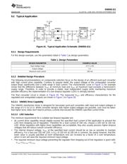
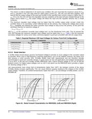
9.2.2.4 Capacitor Selection
The capacitors in the converter circuit in Figure 45 are multi-layer ceramic chip (MLCC) capacitors.
As with all high speed CMOS ICs, the SN6501 requires a bypass capacitor in the range of 10 nF to 100 nF.
The input bulk capacitor at the center-tap of the primary supports large currents into the primary during the fast
switching transients. For minimum ripple make this capacitor 1 μF to 10 μF. In a 2-layer PCB design with a
dedicated ground plane, place this capacitor close to the primary center-tap to minimize trace inductance. In a 4-
layer board design with low-inductance reference planes for ground and V
IN
, the capacitor can be placed at the
supply entrance of the board. To ensure low-inductance paths use two vias in parallel for each connection to a
reference plane or to the primary center-tap.
The bulk capacitor at the rectifier output smoothes the output voltage. Make this capacitor 1 μF to 10 μF.
The small capacitor at the regulator input is not necessarily required. However, good analog design practice
suggests, using a small value of 47 nF to 100 nF improves the regulator’s transient response and noise rejection.
The LDO output capacitor buffers the regulated output for the subsequent isolator and transceiver circuitry. The
choice of output capacitor depends on the LDO stability requirements specified in the data sheet. However, in
most cases, a low-ESR ceramic capacitor in the range of 4.7 μF to 10 μF will satisfy these requirements.
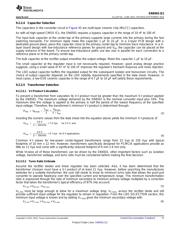
9.2.2.5 Transformer Selection
9.2.2.5.1 V-t Product Calculation
To prevent a transformer from saturation its V-t product must be greater than the maximum V-t product applied
by the SN6501. The maximum voltage delivered by the SN6501 is the nominal converter input plus 10%. The
maximum time this voltage is applied to the primary is half the period of the lowest frequency at the specified
input voltage. Therefore, the transformer’s minimum V-t product is determined through:
(3)
Inserting the numeric values from the data sheet into the equation above yields the minimum V-t products of
(4)
Common V-t values for low-power center-tapped transformers range from 22 Vμs to 150 Vμs with typical
footprints of 10 mm x 12 mm. However, transformers specifically designed for PCMCIA applications provide as
little as 11 Vμs and come with a significantly reduced footprint of 6 mm x 6 mm only.
While Vt-wise all of these transformers can be driven by the SN6501, other important factors such as isolation
voltage, transformer wattage, and turns ratio must be considered before making the final decision.
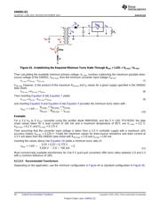
9.2.2.5.2 Turns Ratio Estimate
Assume the rectifier diodes and linear regulator has been selected. Also, it has been determined that the
transformer choosen must have a V-t product of at least 11 Vμs. However, before searching the manufacturer
websites for a suitable transformer, the user still needs to know its minimum turns ratio that allows the push-pull
converter to operate flawlessly over the specified current and temperature range. This minimum transformation
ratio is expressed through the ratio of minimum secondary to minimum primary voltage multiplied by a correction
factor that takes the transformer’s typical efficiency of 97% into account:
V
P-min
= V
IN-min
- V
DS-max
(5)
V
S-min
must be large enough to allow for a maximum voltage drop, V
F-max
, across the rectifier diode and still
provide sufficient input voltage for the regulator to remain in regulation. From the LDO SELECTION section, this
minimum input voltage is known and by adding V
F-max
gives the minimum secondary voltage with:
V
S-min
= V
F-max
+ V
DO-max
+ V
O-max
(6)
Copyright © 2013–2014, Texas Instruments Incorporated Submit Documentation Feedback 17
Product Folder Links: SN6501-Q1
器件 Datasheet 文档搜索
AiEMA 数据库涵盖高达 72,405,303 个元件的数据手册,每天更新 5,000 多个 PDF 文件
