Datasheet 搜索 > 接口芯片 > TI(德州仪器) > SN65HVD12DR 数据手册 > SN65HVD12DR 数据手册 18/37 页
 器件3D模型
¥ 1.555
SN65HVD12DR 数据手册 - TI(德州仪器)
制造商:
TI(德州仪器)
分类:
接口芯片
封装:
SOIC-8
描述:
TEXAS INSTRUMENTS SN65HVD12DR 收发器, RS485, 3V-3.6电源, SOIC-8
Pictures:
3D模型
符号图
焊盘图
引脚图
产品图
页面导航:
引脚图在P3Hot
典型应用电路图在P1P21P22
原理图在P17P18
封装尺寸在P29P30P31P33P34
标记信息在P3P29P30P31
封装信息在P28P29P30P31P32P33P34
技术参数、封装参数在P4
应用领域在P1P32P37
电气规格在P6P7P22
型号编号列表在P3
导航目录
SN65HVD12DR数据手册
Page:
of 37 Go
若手册格式错乱,请下载阅览PDF原文件
SN65HVD10
,
SN65HVD10Q
,
SN75HVD10
,
SN65HVD11
SN65HVD12
,
SN75HVD12
,
SN65HVD11Q
,
SN75HVD11
SLLS505N –FEBRUARY 2002–REVISED JULY 2015
www.ti.com
9 Detailed Description
9.1 Overview
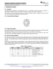
The SN65HVD10, SN65HVD11, and SN65HVD12 are 3.3 V, half-duplex, RS-485 transceivers available in 3
speed grades suitable for data transmission up to 32 Mbps, 10 Mbps, and 1 Mbps, respectively.
These devices have active-high driver enables and active-low receiver enables. A standby current of less than
5 µA can be achieved by disabling both driver and receiver.
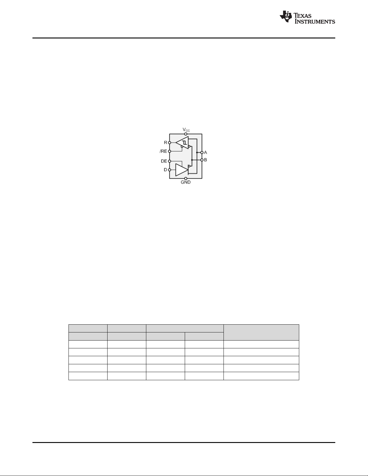
9.2 Functional Block Diagram
9.3 Feature Description
Internal ESD protection circuits protect the transceiver bus terminals against ±16-kV Human Body Model (HBM)
electrostatic discharges and ±4-kV electrical fast transients (EFT) according to IEC61000-4-4.
The SN65HVD1x half-duplex family provides internal biasing of the receiver input thresholds for open-circuit,
bus-idle, or short-circuit failsafe conditions, and a typical receiver hysteresis of 35 mV.
9.4 Device Functional Modes
When the driver enable pin, DE, is logic high, the differential outputs A and B follow the logic states at data input
D. A logic high at D causes A to turn high and B to turn low. In this case the differential output voltage defined as
V
OD
= V
A
– V
B
is positive. When D is low, the output states reverse, B turns high, A becomes low, and V
OD
is
negative.
When DE is low, both outputs turn high-impedance. In this condition the logic state at D is irrelevant. The DE pin
has an internal pulldown resistor to ground; thus, when left open, the driver is disabled (high-impedance) by
default. The D pin has an internal pullup resistor to V
CC
; thus, when left open while the driver is enabled, output A
turns high and B turns low.
Table 1. Driver Functions
(1)
INPUT ENABLE OUTPUTS
FUNCTION
D DE A B
H H H L Actively drive bus High
L H L H Actively drive bus Low
X L Z Z Driver disabled
X OPEN Z Z Driver disabled by default
OPEN H H L Actively drive bus High by default
(1) H = high level; L = low level; Z = high impedance; X = irrelevant; ? = indeterminate
18 Submit Documentation Feedback Copyright © 2002–2015, Texas Instruments Incorporated
Product Folder Links: SN65HVD10 SN65HVD10Q SN75HVD10 SN65HVD11 SN65HVD12 SN75HVD12
SN65HVD11Q SN75HVD11
器件 Datasheet 文档搜索
AiEMA 数据库涵盖高达 72,405,303 个元件的数据手册,每天更新 5,000 多个 PDF 文件
