Datasheet 搜索 > 逻辑控制器 > TI(德州仪器) > SN74AUC1G17DBVRG4 数据手册 > SN74AUC1G17DBVRG4 数据手册 2/18 页

¥ 1.262
SN74AUC1G17DBVRG4 数据手册 - TI(德州仪器)
制造商:
TI(德州仪器)
分类:
逻辑控制器
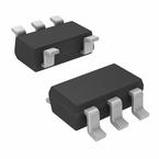
封装:
SOT-23-5
描述:
单路施密特触发缓冲器 5-SOT-23 -40 to 85
Pictures:
3D模型
符号图
焊盘图
引脚图
产品图
页面导航:
导航目录
SN74AUC1G17DBVRG4数据手册
Page:
of 18 Go
若手册格式错乱,请下载阅览PDF原文件
www.ti.com
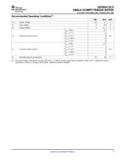
Absolute Maximum Ratings
(1)
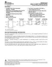
SN74AUC1G17
SINGLE SCHMITT-TRIGGER BUFFER
SCES376N – SEPTEMBER 2001 – REVISED APRIL 2007
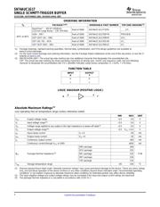
ORDERING INFORMATION
T
A
PACKAGE
(1) (2)
ORDERABLE PART NUMBER TOP-SIDE MARKING
(3)
NanoFree™ – WCSP (DSBGA)
Reel of 3000 SN74AUC1G17YZPR _ _ _U7_
0.23-mm Large Bump – YZP (Pb-free)
SON – DRY Reel of 5000 SN74AUC1G17DRYR PREVIEW
–40 ° C to 85 ° C
SOT (SOT-23) – DBV Reel of 3000 SN74AUC1G17DBVR U17_
SOT (SC-70) – DCK Reel of 3000 SN74AUC1G17DCKR U7_
SOT (SOT-553) – DRL Reel of 4000 SN74AUC1G17DRLR U7_
(1) Package drawings, standard packing quantities, thermal data, symbolization, and PCB design guidelines are available at
www.ti.com/sc/package.
(2) For the most current package and ordering information, see the Package Option Addendum at the end of this document, or see the TI
website at www.ti.com .
(3) DBV/DCK/DRL/DRY: The actual top-side marking has one additional character that designates the assembly/test site.
YZP: The actual top-side marking has three preceding characters to denote year, month, and sequence code, and one following
character to designate the assembly/test site. Pin 1 identifier indicates solder-bump composition (1 = SnPb, • = Pb-free).
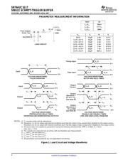
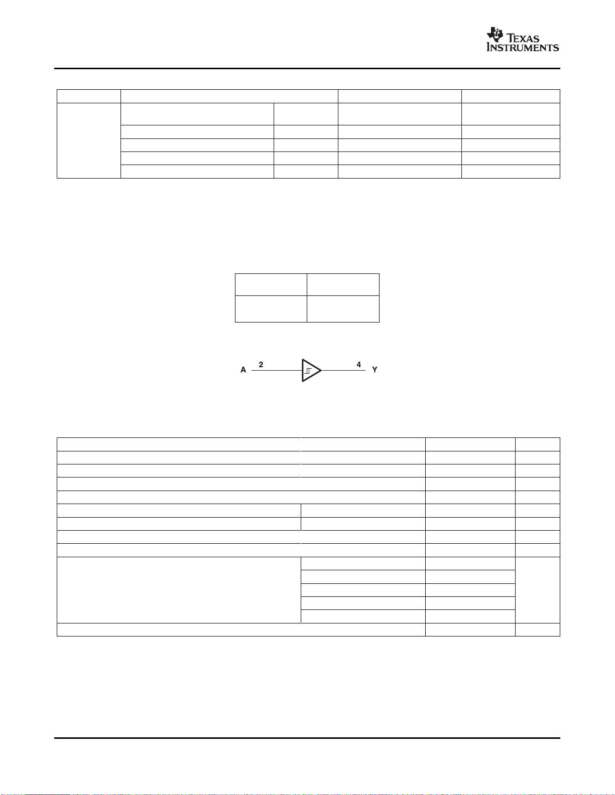
FUNCTION TABLE
INPUT OUTPUT
A Y
H H
L L
LOGIC DIAGRAM (POSITIVE LOGIC)
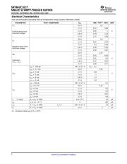
over operating free-air temperature range (unless otherwise noted)
MIN MAX UNIT
V
CC
Supply voltage range –0.5 3.6 V
V
I
Input voltage range
(2)
–0.5 3.6 V
V
O
Voltage range applied to any output in the high impedance or power-off state
(2)
–0.5 3.6 V
V
O
Output voltage range
(2)
–0.5 V
CC
+ 0.5 V
I
IK
Input clamp current V
I
< 0 –50 mA
I
OK
Output clamp current V
O
< 0 –50 mA
I
O
Continuous output current ± 20 mA
Continuous current through V
CC
or GND ± 100 mA
DBV package 206
DCK package 252
θ
JA
Package thermal impedance
(3)
DRL package 142 ° C/W
DRY package 234
YZP package 132
T
stg
Storage temperature range –65 150 ° C
(1) Stresses beyond those listed under "absolute maximum ratings" may cause permanent damage to the device. These are stress ratings
only, and functional operation of the device at these or any other conditions beyond those indicated under "recommended operating
conditions" is not implied. Exposure to absolute-maximum-rated conditions for extended periods may affect device reliability.
(2) The input negative-voltage and output voltage ratings may be exceeded if the input and output current ratings are observed.
(3) The package thermal impedance is calculated in accordance with JESD 51-7.
2
Submit Documentation Feedback
器件 Datasheet 文档搜索
AiEMA 数据库涵盖高达 72,405,303 个元件的数据手册,每天更新 5,000 多个 PDF 文件
