Datasheet 搜索 > 电压电平转换器 > TI(德州仪器) > SN74AVCH4T245RGYR 数据手册 > SN74AVCH4T245RGYR 数据手册 17/37 页

¥ 8.15
SN74AVCH4T245RGYR 数据手册 - TI(德州仪器)
制造商:
TI(德州仪器)
分类:
电压电平转换器
封装:
VQFN-16
描述:
可配置电压转换和三态输出的4位双电源总线收发器 4-BIT DUAL-SUPPLY BUS TRANSCEIVER WITH CONFIGURABLE VOLTAGE TRANSLATION AND 3-STATE OUTPUTS
Pictures:
3D模型
符号图
焊盘图
引脚图
产品图
页面导航:
引脚图在P4Hot
典型应用电路图在P1P17P19P20
原理图在P17
封装尺寸在P24P26P27
焊盘布局在P22
标记信息在P24P25
封装信息在P23P24P25P26P27
技术参数、封装参数在P5
应用领域在P1P17P23P25P37
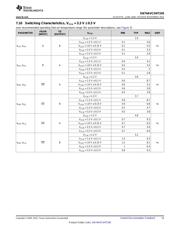
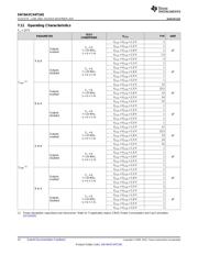
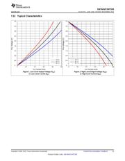
电气规格在P7P8P18
导航目录
SN74AVCH4T245RGYR数据手册
Page:
of 37 Go
若手册格式错乱,请下载阅览PDF原文件
DIR
OE
A1
A2
B1
B2
SN74AVCH4T245
www.ti.com
SCES577E –JUNE 2004–REVISED NOVEMBER 2015
9 Detailed Description
9.1 Overview
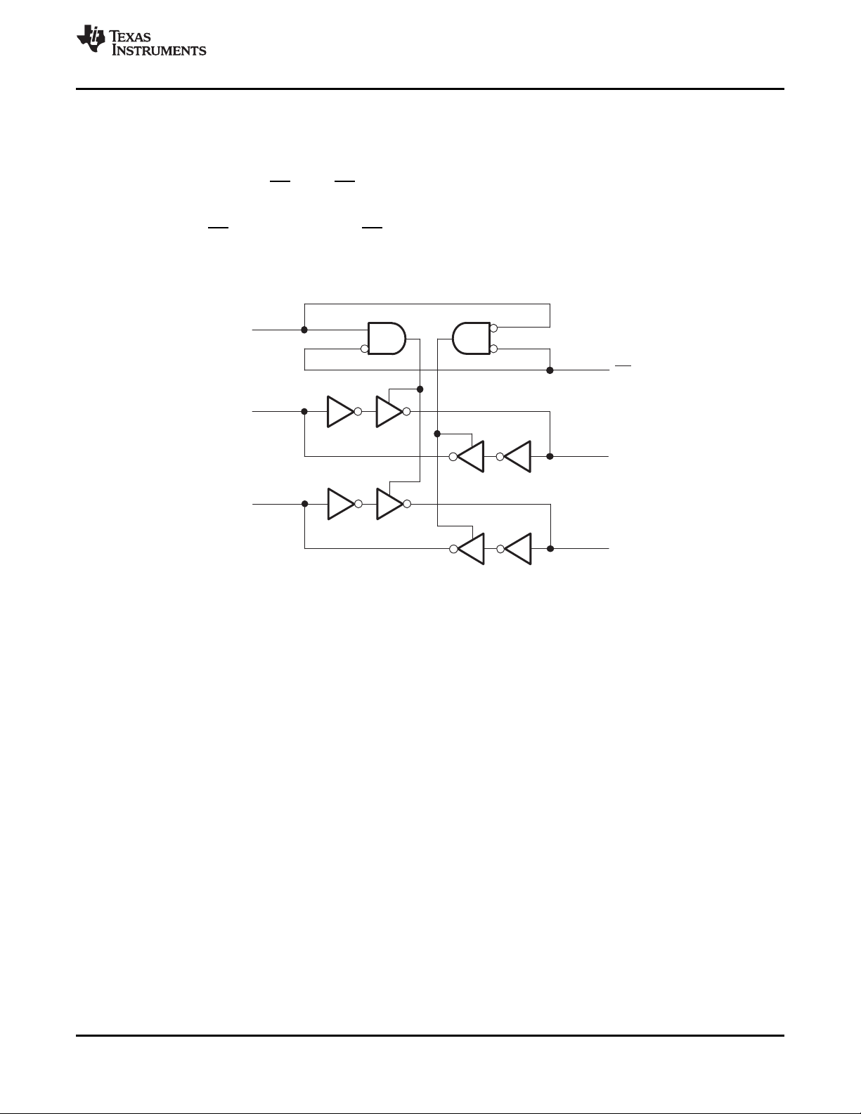
The SN74AVCH4T245 is a 4-bit, dual-supply noninverting bidirectional voltage level translation device. Ax pins
and control pins (1DIR, 2DIR,1OE, and 2OE) are supported by V
CCA
, and Bx pins are supported by V
CCB
. The A
port is able to accept I/O voltages ranging from 1.2 V to 3.6 V, while the B port can accept I/O voltages from 1.2
V to 3.6 V. A high on DIR allows data transmission from Ax to Bx and a low on DIR allows data transmission
from Bx to Ax when OE is set to low. When OE is set to high, both Ax and Bx pins are in the high-impedance
state. Refer to the AVC Logic Family Technology and Applications Application Report SCEA006).
9.2 Functional Block Diagram
Figure 4. Logic Diagram (Positive Logic) for 1/2 of SN74AVCH4T245
9.3 Feature Description
9.3.1 Fully Configurable Dual-Rail Design Allows Each Port to Operate Over the Full 1.2V to 3.6V Power-
Supply Range
Both V
CCA
and V
CCB
can be supplied at any voltage between 1.2 V and 3.6 V; thus, making the device suitable
for translating between any of the low voltage nodes (1.2 V, 1.8 V, 2.5 V, and 3.3 V).
9.3.2 Supports High Speed Translation
The SN74AVCH4T245 device can support high data rate applications. The translated signal data rate can be up
to 380 Mbps when the signal is translated from 1.8 V to 3.3 V.
9.3.3 I
off
Supports Partial-Power-Down Mode Operation
I
off
will prevent backflow current by disabling I/O output circuits when device is in partial-power-down mode.
9.3.4 Bus-Hold Circuitry
This device has active bus-hold circuitry that holds unused or undriven inputs at a valid logic state. Use of pull-up
or pull-down resistors with the bus-hold circuitry is not recommended. (Refer to the Bus-Hold Circuit Application
Report (SCLA015). Pullup and pulldown resistors are not recommended on the inputs of devices with bus-hold.
Unused inputs can be left floating.
Copyright © 2004–2015, Texas Instruments Incorporated Submit Documentation Feedback 17
Product Folder Links: SN74AVCH4T245
器件 Datasheet 文档搜索
AiEMA 数据库涵盖高达 72,405,303 个元件的数据手册,每天更新 5,000 多个 PDF 文件
