Datasheet 搜索 > TI(德州仪器) > SN74CB3Q3125 数据手册 > SN74CB3Q3125 数据手册 1/25 页

¥ 0
SN74CB3Q3125 数据手册 - TI(德州仪器)
制造商:
TI(德州仪器)
描述:
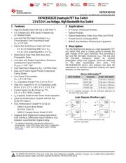
四路 FET、2.5V/3.3V、低压高带宽总线开关
Pictures:
3D模型
符号图
焊盘图
引脚图
产品图
页面导航:
引脚图在P3Hot
典型应用电路图在P1P10P11
原理图在P8
封装尺寸在P14P16P17
标记信息在P14P15
封装信息在P13P14P15P16P17
技术参数、封装参数在P4P11
应用领域在P1
电气规格在P5
型号编号列表在P11
导航目录
SN74CB3Q3125数据手册
Page:
of 25 Go
若手册格式错乱,请下载阅览PDF原文件
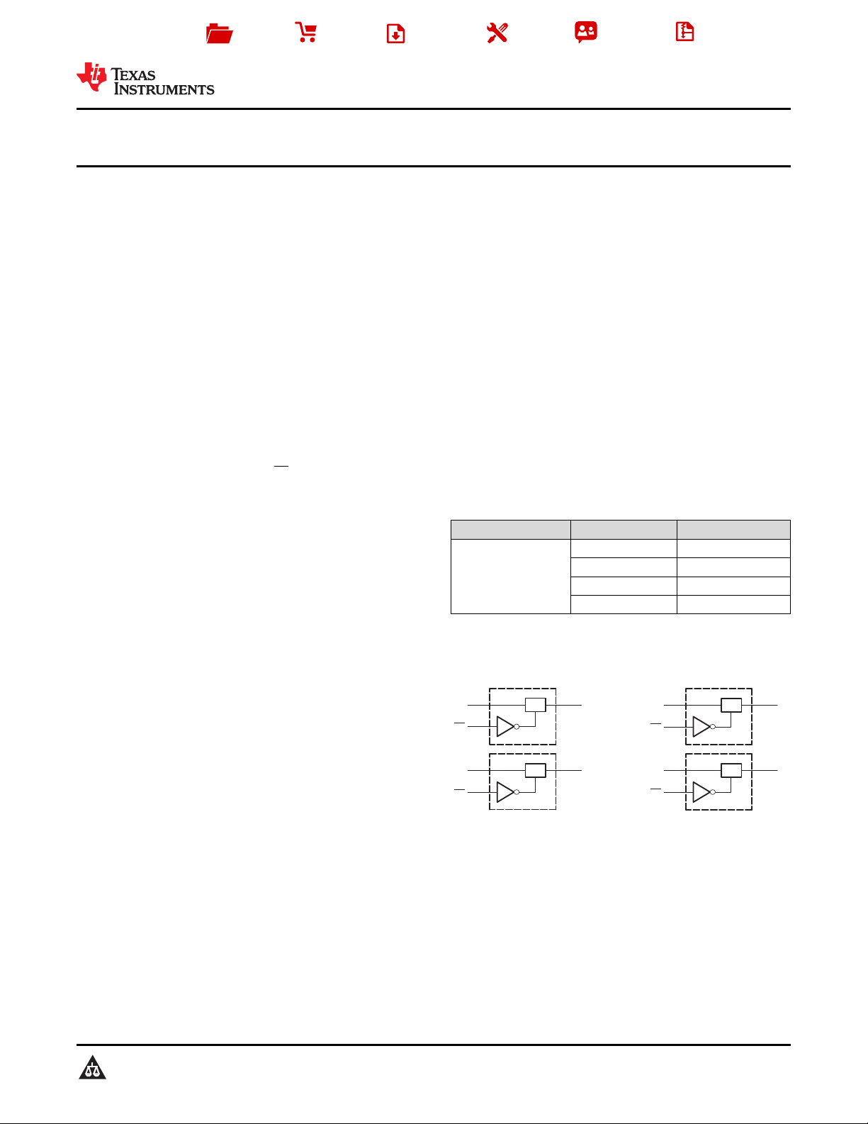
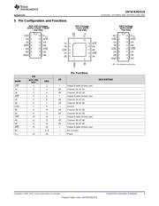
1A
1OE
SW
1B
3A
3OE
SW
3B
2A
2OE
SW
2B
4A
4OE
SW
4B
2
1
9
10
3
8
5
4
12
13
6
11
Product
Folder
Sample &
Buy
Technical
Documents
Tools &
Software
Support &
Community
Reference
Design
SN74CB3Q3125
SCDS143C –OCTOBER 2003–REVISED JUNE 2015
SN74CB3Q3125 Quadruple FET Bus Switch
2.5-V/3.3-V Low-Voltage, High-Bandwidth Bus Switch
1 Features 2 Applications
1
• High-Bandwidth Data Path (up to 500 MHz
(1)
)
• IP Phones: Wired and Wireless
• 5-V Tolerant I/Os With Device Powered Up • Optical Modules
or Powered Down
• Optical Networking: Video Over Fiber and EPON
• Low and Flat ON-State Resistance (r
on
)
• Private Branch Exchange (PBX)
Characteristics Over Operating Range
• WiMAX and Wireless Infrastructure Equipment
(r
on
= 3 Ω Typ)
• Rail-to-Rail Switching on Data I/O Ports
3 Description
– 0-V to 5-V Switching With 3.3-V V
CC
The SN74CB3Q3125 device is a high-bandwidth FET
bus switch that uses a charge pump to elevate the
– 0-V to 3.3-V Switching With 2.5-V V
CC
gate voltage of the pass transistor, thus providing a
• Bidirectional Data Flow With Near-Zero
low and flat ON-state resistance (r
on
). The low and
Propagation Delay
flat ON-state resistance allows for minimal
• Low Input and Output Capacitance Minimizes
propagation delay and supports rail-to-rail switching
Loading and Signal Distortion
on the data input/output (I/O) ports. The
SN74CB3Q3125 device also features low data I/O
(C
io(OFF)
= 4 pF Typ)
capacitance to minimize capacitive loading and signal
• Fast Switching Frequency (f
OE
= 20 MHz Max)
distortion on the data bus.
• Data and Control Inputs Provide Undershoot
Clamp Diodes
Device Information
(1)
• Low Power Consumption
PART NUMBER PACKAGE BODY SIZE (NOM)
(I
CC
= 0.3 mA Typ)
VQFN (14) 3.50 mm × 3.50 mm
• V
CC
Operating Range From 2.3 V to 3.6 V
SSOP (16) 4.90 mm × 3.90 mm
SN74CB3Q3125
• Data I/Os Support 0-V to 5-V Signaling Levels
TSSOP (16) 5.00 mm × 4.40 mm
(0.8 V, 1.2 V, 1.5 V, 1.8 V, 2.5 V, 3.3 V, 5 V)
TVSOP (16) 4.40 mm × 3.60 mm
• Control Inputs Can Be Driven by TTL,
(1) For all available packages, see the orderable addendum at
5-V, or 3.3-V CMOS Outputs
the end of the data sheet.
• I
off
Supports Partial-Power-Down Mode Operation
Logic Diagram (Positive Logic)
• Latch-Up Performance Exceeds 100 mA Per
JESD 78, Class II
• ESD Performance Tested Per JESD 22
– 2000-V Human-Body Model
(A114-B, Class II)
– 1000-V Charged-Device Model (C101)
• Supports Both Digital and Analog Applications:
USB Interface, Differential Signal Interface, Bus
Pin numbers shown are for the DGV, PW,
Isolation, Low-Distortion Signal Gating
and RGY packages.
(1)
For additional information regarding the performance
characteristics of the CB3Q family, refer to the TI application
report, CBT-C, CB3T, and CB3Q Signal-Switch Families
(SCDA008).
1
An IMPORTANT NOTICE at the end of this data sheet addresses availability, warranty, changes, use in safety-critical applications,
intellectual property matters and other important disclaimers. PRODUCTION DATA.
器件 Datasheet 文档搜索
AiEMA 数据库涵盖高达 72,405,303 个元件的数据手册,每天更新 5,000 多个 PDF 文件
