Datasheet 搜索 > 逻辑控制器 > TI(德州仪器) > SN74CB3Q3125DBQR 数据手册 > SN74CB3Q3125DBQR 数据手册 8/26 页
 器件3D模型
¥ 8.433
SN74CB3Q3125DBQR 数据手册 - TI(德州仪器)
制造商:
TI(德州仪器)
分类:
逻辑控制器
封装:
SSOP-16
描述:
翻两番FET总线开关2.5 -V / 3.3 V低压高带宽总线开关 QUADRUPLE FET BUS SWITCH 2.5-V/3.3-V LOW-VOLTAGE HIGH-BANDWIDTH BUS SWITCH
Pictures:
3D模型
符号图
焊盘图
引脚图
产品图
页面导航:
引脚图在P3Hot
典型应用电路图在P1P10P11
原理图在P8
封装尺寸在P14P16P17
标记信息在P14P15
封装信息在P13P14P15P16P17
技术参数、封装参数在P4P11
应用领域在P1P26
电气规格在P5
型号编号列表在P11


导航目录
SN74CB3Q3125DBQR数据手册
Page:
of 26 Go
若手册格式错乱,请下载阅览PDF原文件
1A
1OE
SW
1B
3A
3OE
SW
3B
2A
2OE
SW
2B
4A
4OE
SW
4B
2
1
9
10
3
8
5
4
12
13
6
11
A
EN
(1)
B
Charge
Pump
V
CC
SN74CB3Q3125
SCDS143C –OCTOBER 2003–REVISED JUNE 2015
www.ti.com
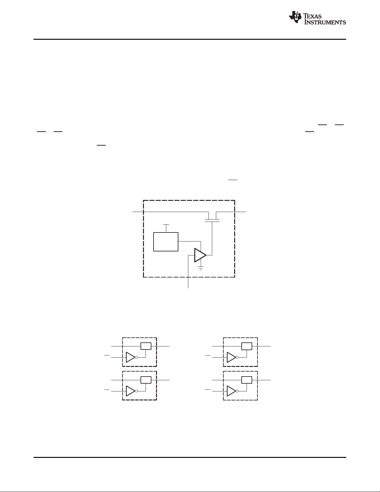
8 Detailed Description
8.1 Overview
The SN74CB3Q3125 device is a high-bandwidth FET bus switch utilizing a charge pump to elevate the gate
voltage of the pass transistor, providing a low and flat ON-state resistance (r
on
). The low and flat ON-state
resistance allows for minimal propagation delay and supports rail-to-rail switching on the data input/output (I/O)
ports. The SN74CB3Q3125 device also features low data I/O capacitance to minimize capacitive loading and
signal distortion on the data bus. Specifically designed to support high-bandwidth applications, the
SN74CB3Q3125 device provides an optimized interface solution ideally suited for broadband communications,
networking, and data-intensive computing systems.
The SN74CB3Q3125 device is organized as four 1-bit bus switches with separate output-enable (1OE, 2OE,
3OE, 4OE) inputs. It can be used as four 1-bit bus switches or as one 4-bit bus switch. When OE is low, the
associated 1-bit bus switch is ON, and the A port is connected to the B port, allowing bidirectional data flow
between ports. When OE is high, the associated 1-bit bus switch is OFF, and a high-impedance state exists
between the A and B ports.
This device is fully specified for partial-power-down applications using I
off
. The I
off
circuitry prevents damaging
current backflow through the device when it is powered down. The device has isolation during power off.
To ensure the high-impedance state during power up or power down, OE should be tied to V
CC
through a pullup
resistor; the minimum value of the resistor is determined by the current-sinking capability of the driver.
Figure 4. Simplified Schematic, Each FET Switch (SW)
8.2 Functional Block Diagram
8 Submit Documentation Feedback Copyright © 2003–2015, Texas Instruments Incorporated
Product Folder Links: SN74CB3Q3125
器件 Datasheet 文档搜索
AiEMA 数据库涵盖高达 72,405,303 个元件的数据手册,每天更新 5,000 多个 PDF 文件
