Datasheet 搜索 > TI(德州仪器) > SN74CB3T16212 数据手册 > SN74CB3T16212 数据手册 1/19 页
 器件3D模型
¥ 0
SN74CB3T16212 数据手册 - TI(德州仪器)
制造商:
TI(德州仪器)
封装:
TSSOP-56
描述:
24 位 FET 总线交换器,具有 5V 容限电平转换器的 2.5V/3.3V 低电压总线开关
Pictures:
3D模型
符号图
焊盘图
引脚图
产品图
页面导航:
典型应用电路图在P4
原理图在P5
封装尺寸在P2P9P11P12P13P16
焊盘布局在P14P17
型号编码规则在P1P2
标记信息在P2P9
封装信息在P2P9P10P11P12
技术参数、封装参数在P5
应用领域在P1
电气规格在P6
导航目录
SN74CB3T16212数据手册
Page:
of 19 Go
若手册格式错乱,请下载阅览PDF原文件
www.ti.com
FEATURES
1
2
3
4
5
6
7
8
9
10
11
12
13
14
15
16
17
18
19
20
21
22
23
24
25
26
27
28
56
55
54
53
52
51
50
49
48
47
46
45
44
43
42
41
40
39
38
37
36
35
34
33
32
31
30
29
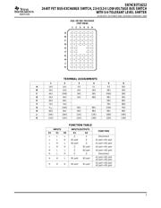
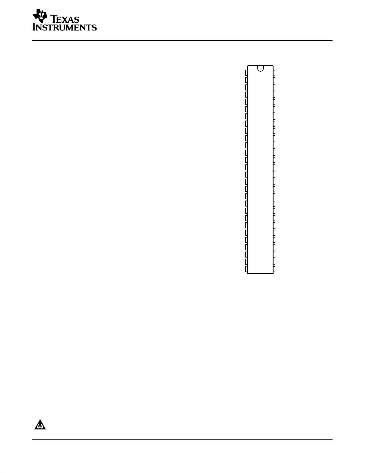
S0
1A1
1A2
2A1
2A2
3A1
3A2
GND
4A1
4A2
5A1
5A2
6A1
6A2
7A1
7A2
V
CC
8A1
GND
8A2
9A1
9A2
10A1
10A2
11A1
11A2
12A1
12A2
S1
S2
1B1
1B2
2B1
2B2
3B1
GND
3B2
4B1
4B2
5B1
5B2
6B1
6B2
7B1
7B2
8B1
GND
8B2
9B1
9B2
10B1
10B2
11B1
11B2
12B1
12B2
DGG OR DGV PACKAGE
(TOP VIEW)
DESCRIPTION/ORDERING INFORMATION
SN74CB3T16212
24-BIT FET BUS-EXCHANGE SWITCH, 2.5-V/3.3-V LOW-VOLTAGE BUS SWITCH
WITH 5-V-TOLERANT LEVEL SHIFTER
SCDS157A – OCTOBER 2003 – REVISED FEBRUARY 2005
• Member of the Texas Instruments Widebus™
Family
• Output Voltage Translation Tracks V
CC
• Supports Mixed-Mode Signal Operation on All
Data I/O Ports
– 5-V Input Down to 3.3-V Output Level Shift
With 3.3-V V
CC
– 5-V/3.3-V Input Down to 2.5-V Output Level
Shift With 2.5-V V
CC
• 5-V-Tolerant I/Os With Device Powered Up or
Powered Down
• Bidirectional Data Flow, With Near-Zero
Propagation Delay
• Low ON-State Resistance (r
on
) Characteristics
(r
on
= 5 Ω Typ)
• Low Input/Output Capacitance Minimizes
Loading (C
io(OFF)
= 9 pF Typ)
• Data and Control Inputs Provide Undershoot
Clamp Diodes
• Low Power Consumption (I
CC
= 70 µ A Max)
• V
CC
Operating Range From 2.3 V to 3.6 V
• Data I/Os Support 0-V to 5-V Signaling Levels
(0.8 V, 1.2 V, 1.5 V, 1.8 V, 2.5 V, 3.3 V, 5 V)
• Control Inputs Can Be Driven by TTL or
5-V/3.3-V CMOS Outputs
• I
off
Supports Partial-Power-Down Mode
Operation
• Latch-Up Performance Exceeds 250 mA Per
JESD 17
• ESD Performance Tested Per JESD 22
– 2000-V Human-Body Model(A114-B, Class II)
– 1000-V Charged-Device Model (C101)
• Supports Digital Applications: Level
Translation, PCI Interface, USB Interface,
Memory Interleaving, and Bus Isolation
• Ideal for Low-Power Portable Equipment
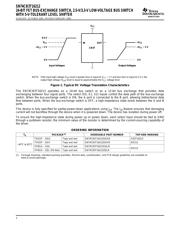
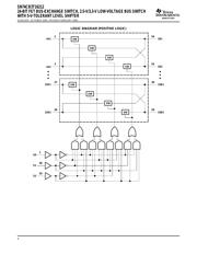
The SN74CB3T16212 is a high-speed TTL-compatible FET bus-exchange switch, with low ON-state resistance
(r
on
), allowing for minimal propagation delay. The device fully supports mixed-mode signal operation on all data
I/O ports by providing voltage translation that tracks V
CC
. The SN74CB3T16212 supports systems using 5-V TTL,
3.3-V LVTTL, and 2.5-V CMOS switching standards, as well as user-defined switching levels (see Figure 1).
Please be aware that an important notice concerning availability, standard warranty, and use in critical applications of Texas
Instruments semiconductor products and disclaimers thereto appears at the end of this data sheet.
Widebus is a trademark of Texas Instruments.
PRODUCTION DATA information is current as of publication date.
Copyright © 2003–2005, Texas Instruments Incorporated
Products conform to specifications per the terms of the Texas
Instruments standard warranty. Production processing does not
necessarily include testing of all parameters.
器件 Datasheet 文档搜索
AiEMA 数据库涵盖高达 72,405,303 个元件的数据手册,每天更新 5,000 多个 PDF 文件
