Datasheet 搜索 > 逻辑芯片 > TI(德州仪器) > SN74LV1T125DBVR 数据手册 > SN74LV1T125DBVR 数据手册 6/20 页

¥ 0.683
SN74LV1T125DBVR 数据手册 - TI(德州仪器)
制造商:
TI(德州仪器)
分类:
逻辑芯片
封装:
SOT-23-5
描述:
具有三态输出的单电源单路缓冲门(低电平有效) 5-SOT-23 -40 to 125
Pictures:
3D模型
符号图
焊盘图
引脚图
产品图
页面导航:
导航目录
SN74LV1T125DBVR数据手册
Page:
of 20 Go
若手册格式错乱,请下载阅览PDF原文件
SN74LV1T125
SCLS745A –DECEMBER 2013–REVISED FEBRUARY 2014
www.ti.com
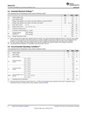
4.3 Absolute Maximum Ratings
(1)
over operating free-air temperature range (unless otherwise noted)
MIN MAX UNIT
V
CC
Supply voltage range –0.5 7.0 V
V
I
Input voltage range
(2)
–0.5 7.0 V
Voltage range applied to any output in the high-impedance or power-off state
(2)
–0.5 4.6 V
V
O
Voltage range applied to any output in the high or low state
(2)
–0.5 V
CC
+ 0.5 V
I
IK
Input clamp current V
I
< 0 –20 mA
I
OK
Output clamp current V
O
< 0 or V
O
> V
CC
±20 mA
I
O
Continuous output current ±25 mA
Continuous current through V
CC
or GND ±50 mA
DBV package 206
Package thermal
θ
JA
°C/W
impedance
(3)
DCK package 252
T
stg
Storage temperature range –65 150 °C
(1) Stresses beyond those listed under "absolute maximum ratings" may cause permanent damage to the device. These are stress ratings
only, and functional operation of the device at these or any other conditions beyond those indicated under "recommended operating
conditions" is not implied. Exposure to absolute-maximum-rated conditions for extended periods may affect device reliability.
(2) The input negative-voltage and output voltage ratings may be exceeded if the input and output current ratings are observed.
(3) The package thermal impedance is calculated in accordance with JESD 51-7.
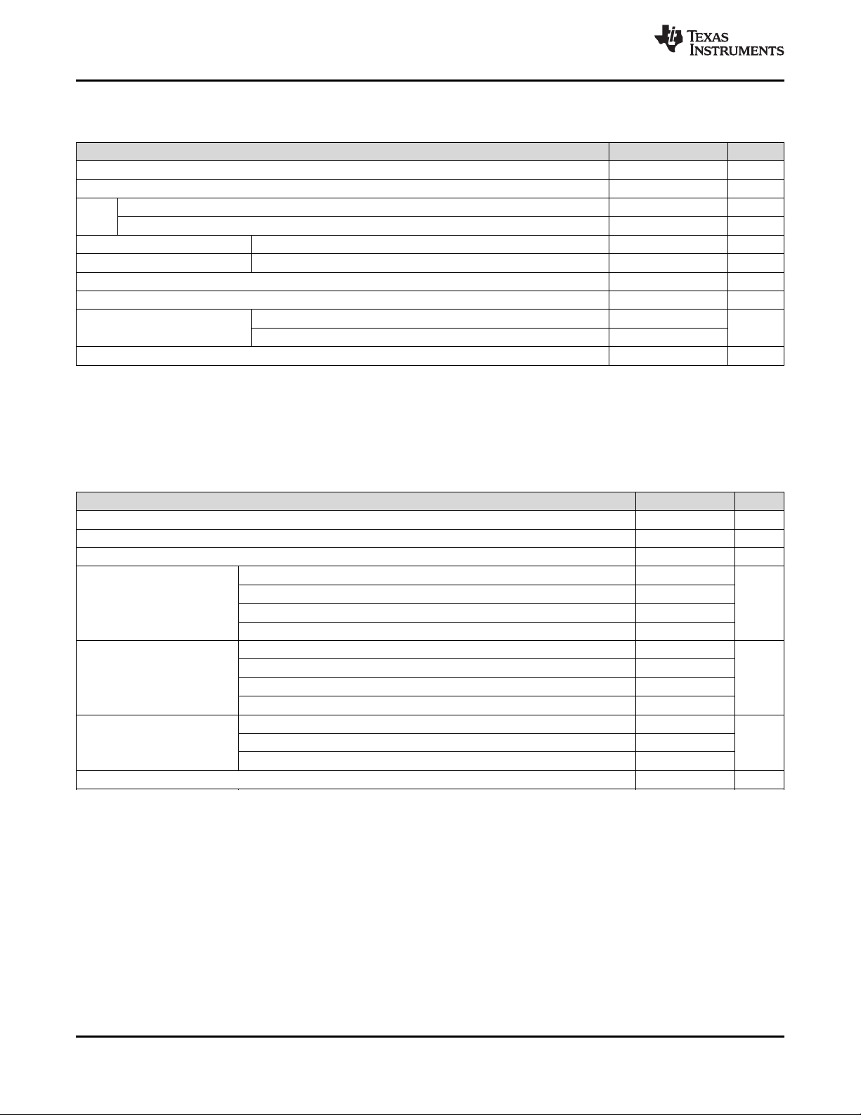
4.4 Recommended Operating Conditions
(1)
over operating free-air temperature range (unless otherwise noted)
MIN MAX UNIT
V
CC
Supply voltage 1.6 5.5 V
V
I
Input voltage 0 5.5 V
V
O
Output voltage 0 V
CC
V
V
CC
= 1.8 V –3.0
V
CC
= 2.5 V –5.0
High-level output
I
OH
mA
current
V
CC
= 3.3 V –7.0
V
CC
= 5.0 V –8.0
V
CC
= 1.8 V 3.0
V
CC
= 2.5 V 5.0
Low-level output
I
OL
mA
current
V
CC
= 3.3 V 7.0
V
CC
= 5.0 V 8.0
V
CC
= 1.8 V 20
Input transition rise or
Δt/Δv V
CC
= 3.3 V or 2.5 V 20 ns/V
fall rate
V
CC
= 5.0 V 20
T
A
Operating free-air temperature –40 125 °C
(1) All unused inputs of the device must be held at V
CC
or GND to ensure proper device operation. Refer to the TI application report,
Implications of Slow or Floating CMOS Inputs, literature number SCBA004.
6 Submit Documentation Feedback Copyright © 2013–2014, Texas Instruments Incorporated
Product Folder Links: SN74LV1T125
器件 Datasheet 文档搜索
AiEMA 数据库涵盖高达 72,405,303 个元件的数据手册,每天更新 5,000 多个 PDF 文件
