Datasheet 搜索 > TI(德州仪器) > SN74LVC1G139DCT 数据手册 > SN74LVC1G139DCT 数据手册 10/22 页


¥ 0
SN74LVC1G139DCT 数据手册 - TI(德州仪器)
制造商:
TI(德州仪器)
Pictures:
3D模型
符号图
焊盘图
引脚图
产品图
页面导航:
引脚图在P3Hot
典型应用电路图在P10P11
原理图在P1P9
封装尺寸在P13P15P16
标记信息在P13P14
封装信息在P12P13P14P15P16
技术参数、封装参数在P3
应用领域在P1P22
电气规格在P5

导航目录
SN74LVC1G139DCT数据手册
Page:
of 22 Go
若手册格式错乱,请下载阅览PDF原文件
VCC
Chip Select 2
Address line 14
Chip Select 3
GND Plane
Address line 15
6
5
7
1
2
3
4
8
PF
A
B
Y3
GND
VCC
Y0
Y1
Y2
GND
Chip Select 1
Chip Select 0
SN74LVC1G139
SN74LVC1G139
SCES602D –AUGUST 2004–REVISED AUGUST 2015
www.ti.com
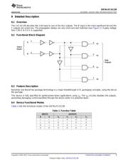
9 Application and Implementation
NOTE
Information in the following applications sections is not part of the TI component
specification, and TI does not warrant its accuracy or completeness. TI’s customers are
responsible for determining suitability of components for their purposes. Customers should
validate and test their design implementation to confirm system functionality.
9.1 Application Information
The SN74LVC1G139 device is a 2-of-4 decoder and demultiplexer. This device decodes the 2-bit address on
inputs A (bit 0) and B (bit 1) then provides a logic low on the matching address output. It can produce 24 mA of
drive current at 3.3 V, making it ideal for driving multiple outputs.
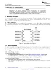
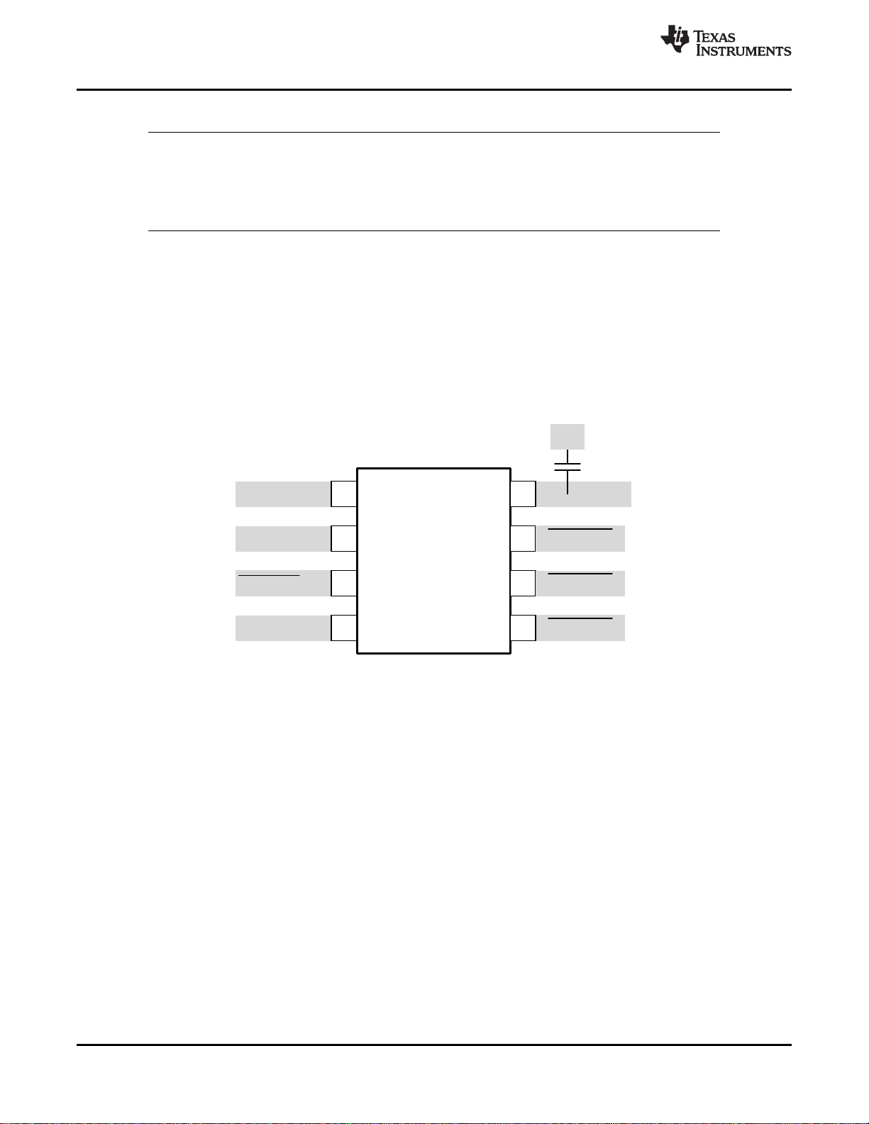
9.2 Typical Application
This is an address line decoder using a 16-bit bus example; address bus lines 14 and 15 are decoded and drive
four active low chip selects. Each output covers 16k address space mapped by the address bus lines 0 through
13.
Figure 4. Typical Application Diagram
9.2.1 Design Requirements
This device uses CMOS technology and has balanced output drive. Take care to avoid bus contention because it
can drive currents that would exceed maximum limits. Outputs can be combined to produce higher drive but the
high drive will also create faster edges into light loads so routing and load conditions should be considered to
prevent ringing.
9.2.2 Detailed Design Procedure
1. Recommended Input Conditions:
– For rise time and fall time specifications, see (Δt/ΔV) in Recommended Operating Conditions table.
– For specified high and low levels, see (V
IH
and V
IL
) in Recommended Operating Conditions table.
– Inputs are overvoltage tolerant allowing them to go as high as 5.5 V at any valid V
CC
.
2. Recommend Output Conditions:
– Load currents should not exceed 50 mA per output and 100 mA total for the part.
– Series resistors on the output may be used if the user desires to slow the output edge signal or limit the
output current.
10 Submit Documentation Feedback Copyright © 2004–2015, Texas Instruments Incorporated
Product Folder Links: SN74LVC1G139
器件 Datasheet 文档搜索
AiEMA 数据库涵盖高达 72,405,303 个元件的数据手册,每天更新 5,000 多个 PDF 文件
