Datasheet 搜索 > 逻辑芯片 > TI(德州仪器) > SN74LVC1G32DCKR 数据手册 > SN74LVC1G32DCKR 数据手册 10/38 页
 器件3D模型
¥ 0.189
SN74LVC1G32DCKR 数据手册 - TI(德州仪器)
制造商:
TI(德州仪器)
分类:
逻辑芯片
封装:
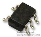
SC-70-5
描述:
TEXAS INSTRUMENTS SN74LVC1G32DCKR 或门, LVC系列, 1门, 2输入, 32 mA, 1.65V至5.5V, SC-70-5
Pictures:
3D模型
符号图
焊盘图
引脚图
产品图
页面导航:
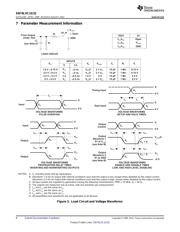
引脚图在P3Hot
典型应用电路图在P11P12
原理图在P10
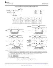
封装尺寸在P14P15P17P18
标记信息在P14P15
封装信息在P13P14P15P16P17P18
技术参数、封装参数在P4P11
应用领域在P1P16P38
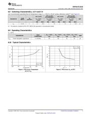
电气规格在P6
型号编号列表在P11
导航目录
SN74LVC1G32DCKR数据手册
Page:
of 38 Go
若手册格式错乱,请下载阅览PDF原文件
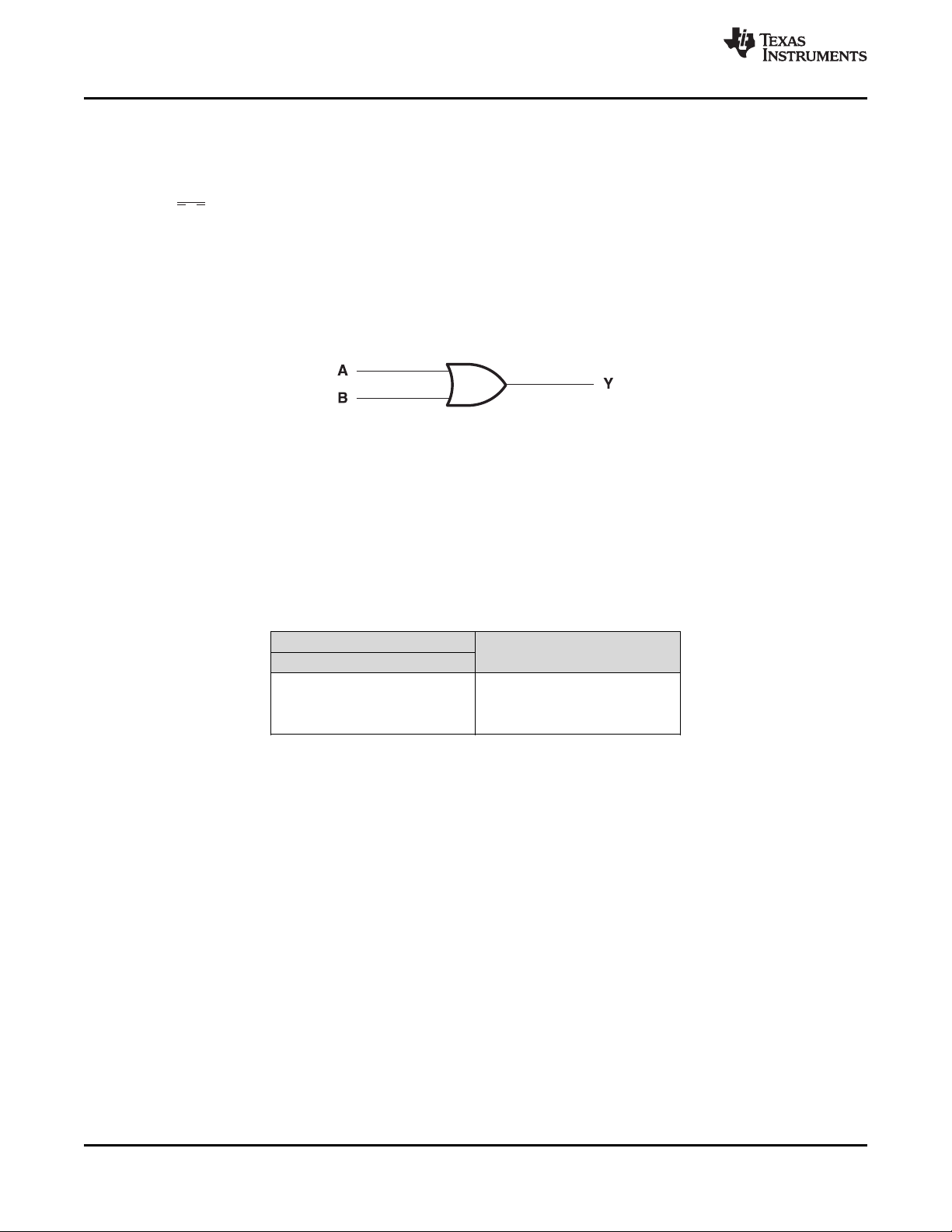
Y = A + B or Y = •A B
SN74LVC1G32
SCES219V –APRIL 1999–REVISED AUGUST 2015
www.ti.com
8 Detailed Description
8.1 Overview
The SN74LVC1G32 device contains one 2-input positive OR gate device and performs the Boolean function
. This device is fully specified for partial-power-down applications using I
off
. The I
off
circuitry
disables the outputs, preventing damaging current backflow through the device when it is powered down.
The DPW package technology is a major breakthrough in IC packaging. Its tiny 0.64 mm square footprint saves
significant board space over other package options while still retaining the traditional manufacturing friendly lead
pitch of 0.5 mm.
8.2 Functional Block Diagram
8.3 Feature Description
• Wide operating voltage range.
– Operates from 1.65 V to 5.5 V.
• Allows down voltage translation.
• Inputs accept voltages to 5.5 V.
• I
off
feature allows voltages on the inputs and outputs, when V
CC
is 0 V.
8.4 Device Functional Modes
Function Table
INPUTS
OUTPUT
Y
A B
H X H
X H H
L L L
10 Submit Documentation Feedback Copyright © 1999–2015, Texas Instruments Incorporated
Product Folder Links: SN74LVC1G32
器件 Datasheet 文档搜索
AiEMA 数据库涵盖高达 72,405,303 个元件的数据手册,每天更新 5,000 多个 PDF 文件
